- 您现在的位置:买卖IC网 > PDF目录17063 > DC575A (Linear Technology)BOARD DELTA SIGMA ADC LTC2410 PDF资料下载
参数资料
| 型号: | DC575A |
| 厂商: | Linear Technology |
| 文件页数: | 22/48页 |
| 文件大小: | 0K |
| 描述: | BOARD DELTA SIGMA ADC LTC2410 |
| 软件下载: | QuikEval System |
| 设计资源: | DC575A Design File DC575A Schematic |
| 标准包装: | 1 |
| 系列: | QuikEval™ |
| ADC 的数量: | 2 |
| 位数: | 24 |
| 采样率(每秒): | 7.5 |
| 数据接口: | MICROWIRE?,串行,SPI? |
| 工作温度: | 0°C ~ 70°C |
| 已用 IC / 零件: | LTC2410 |
| 已供物品: | 板 |
| 相关产品: | DC590B-ND - BOARD DEMO USB SERIAL CONTROLLER LTC2410IGN#PBF-ND - IC ADC 24BIT DIFF INP/REF 16SSOP LTC2410CGN#TRPBF-ND - IC ADC 24BIT DIFF INP/REF 16SSOP LTC2410IGN#TRPBF-ND - IC ADC 24BIT DIFF INP/REF 16SSOP LTC2410CGN#PBF-ND - IC ADC 24BIT DIFF INP/REF 16SSOP LTC2410CGN#TR-ND - IC ADC 24BIT DIFF INP/REF 16SSOP LTC2410IGN#TR-ND - IC ADC 24BIT DIFF INP/REF 16SSOP LTC2410IGN-ND - IC A/D CONV 24BIT MICRPWR 16SSOP LTC2410CGN-ND - IC ADC 24BIT DIFF INP/REF 16SSOP |
第1页第2页第3页第4页第5页第6页第7页第8页第9页第10页第11页第12页第13页第14页第15页第16页第17页第18页第19页第20页第21页当前第22页第23页第24页第25页第26页第27页第28页第29页第30页第31页第32页第33页第34页第35页第36页第37页第38页第39页第40页第41页第42页第43页第44页第45页第46页第47页第48页
LTC2410
29
APPLICATIO S I FOR ATIO
WU
U
The magnitude of the dynamic reference current depends
upon the size of the very stable internal sampling capaci-
tors and upon the accuracy of the converter sampling
clock. The accuracy of the internal clock over the entire
temperature and power supply range is typical better than
0.5%. Such a specification can also be easily achieved by
an external clock. When relatively stable resistors
(50ppm/
°C) are used for the external source impedance
seen by REF+ and REF–, the expected drift of the dynamic
current gain error will be insignificant (about 1% of its
value over the entire temperature and voltage range). Even
for the most stringent applications a one-time calibration
operation may be sufficient.
In addition to the reference sampling charge, the reference
pins ESD protection diodes have a temperature dependent
leakage current. This leakage current, nominally 1nA
(
±10nA max), results in a small gain error. A 100 source
resistance will create a 0.05
V typical and 0.5V maxi-
mum full-scale error.
Output Data Rate
When using its internal oscillator, the LTC2410 can pro-
duce up to 7.5 readings per second with a notch frequency
of 60Hz (FO = LOW) and 6.25 readings per second with a
notch frequency of 50Hz (FO = HIGH). The actual output
data rate will depend upon the length of the sleep and data
output phases which are controlled by the user and which
can be made insignificantly short. When operated with an
external conversion clock (FO connected to an external
oscillator), the LTC2410 output data rate can be increased
as desired. The duration of the conversion phase is 20510/
fEOSC. If fEOSC = 153600Hz, the converter behaves as if the
internal oscillator is used and the notch is set at 60Hz.
There is no significant difference in the LTC2410 perfor-
mance between these two operation modes.
An increase in fEOSC over the nominal 153600Hz will
translate into a proportional increase in the maximum
output data rate. This substantial advantage is neverthe-
less accompanied by three potential effects, which must
be carefully considered.
First, a change in fEOSC will result in a proportional change
in the internal notch position and in a reduction of the
converter differential mode rejection at the power line
frequency. In many applications, the subsequent perfor-
mance degradation can be substantially reduced by rely-
ing upon the LTC2410’s exceptional common mode rejec-
tion and by carefully eliminating common mode to differ-
ential mode conversion sources in the input circuit. The
user should avoid single-ended input filters and should
maintain a very high degree of matching and symmetry in
the circuits driving the IN+ and IN– pins.
Second, the increase in clock frequency will increase
proportionally the amount of sampling charge transferred
through the input and the reference pins. If large external
input and/or reference capacitors (CIN, CREF) are used, the
previous section provides formulae for evaluating the
effect of the source resistance upon the converter perfor-
mance for any value of fEOSC. If small external input and/
or reference capacitors (CIN, CREF) are used, the effect of
the external source resistance upon the LTC2410 typical
performance can be inferred from Figures 17, 18, 22 and
23 in which the horizontal axis is scaled by 153600/fEOSC.
Third, an increase in the frequency of the external oscilla-
tor above 460800Hz (a more than 3
×increaseintheoutput
data rate) will start to decrease the effectiveness of the
internal autocalibration circuits. This will result in a pro-
gressive degradation in the converter accuracy and linear-
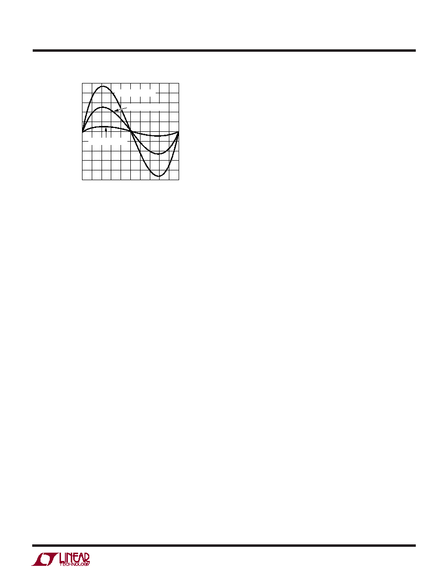
Figure 26. INL vs Differential Input Voltage (VIN = IN+ – IN–)
and Reference Source Resistance (RSOURCE at REF+ and REF– for
Large CREF Values (CREF ≥ 1F)
VINDIF/VREFDIF
–0.5 –0.4–0.3–0.2–0.1 0
0.1 0.2 0.3 0.4 0.5
INL
(ppm
OF
V
REF
)
15
12
9
6
3
0
–3
–6
–9
–12
–15
VCC = 5V
REF+ = 5V
REF– = GND
VINCM = 0.5 (IN
+ + IN–) = 2.5V
FO = GND
CREF = 10F
TA = 25°C
RSOURCE = 1000
RSOURCE = 500
RSOURCE = 100
2410 F26
相关PDF资料 |
PDF描述 |
|---|---|
| MIC2004-1.2YML TR | IC DISTRIBUTION SW 1.2A 6-MLF |
| AD9779A-DPG2-EBZ | BOARD EVALUATION FOR AD9779A |
| DC955A | BOARD DELTA SIGMA ADC LTC2483 |
| SDR0604-181KL | INDUCTOR POWER 180UH 0.38A SMD |
| AP2186SG-13 | IC USB PWR SWITCH 1.5A DUAL 8SOP |
相关代理商/技术参数 |
参数描述 |
|---|---|
| DC579A | 功能描述:BOARD DAC LTC2600 RoHS:是 类别:编程器,开发系统 >> 评估板 - 数模转换器 (DAC) 系列:QuikEval™ 产品培训模块:Lead (SnPb) Finish for COTS Obsolescence Mitigation Program 标准包装:1 系列:- DAC 的数量:4 位数:12 采样率(每秒):- 数据接口:串行,SPI? 设置时间:3µs DAC 型:电流/电压 工作温度:-40°C ~ 85°C 已供物品:板 已用 IC / 零件:MAX5581 |
| DC579A | 制造商:Linear Technology 功能描述:LTC2600 EVALUATION KIT |
| DC57F10W06P6 | 制造商:Conesys 功能描述:CONN 26482 CIRC PIN 6 POS CRMP ST CBL MNT - Bulk |
| DC57F10W06P6-CO | 制造商:Conesys 功能描述:CONN 26482 CIRC PIN 6 POS CRMP ST CBL MNT - Bulk |
| DC57F10W06PN | 制造商:Conesys 功能描述:CONN 26482 CIRC PIN 6 POS CRMP ST CBL MNT - Bulk |
发布紧急采购,3分钟左右您将得到回复。