- 您现在的位置:买卖IC网 > PDF目录17063 > DC682A (Linear Technology)BOARD SAR ADC LTC1859 PDF资料下载
参数资料
| 型号: | DC682A |
| 厂商: | Linear Technology |
| 文件页数: | 16/20页 |
| 文件大小: | 0K |
| 描述: | BOARD SAR ADC LTC1859 |
| 软件下载: | QuikEval System |
| 设计资源: | DC682A Design File DC682A Schematic |
| 标准包装: | 1 |
| 系列: | QuikEval™, SoftSpan™ |
| ADC 的数量: | 1 |
| 位数: | 16 |
| 采样率(每秒): | 100k |
| 数据接口: | MICROWIRE?,串行,SPI? |
| 工作温度: | 0°C ~ 70°C |
| 已用 IC / 零件: | LTC1859 |
| 已供物品: | 板 |
| 相关产品: | LTC1859CG#PBF-ND - IC ADC 8CH 16BIT 100KSPS 28-SSOP LTC1859IG#PBF-ND - IC A/D CONV 8CH 16BIT 28-SSOP LTC1859IG#TRPBF-ND - IC A/D CONV 8CH 16BIT 28-SSOP LTC1859CG#TRPBF-ND - IC A/D CONV 8CH 16BIT 28-SSOP |
LTC1857/LTC1858/LTC1859
5
185789fa
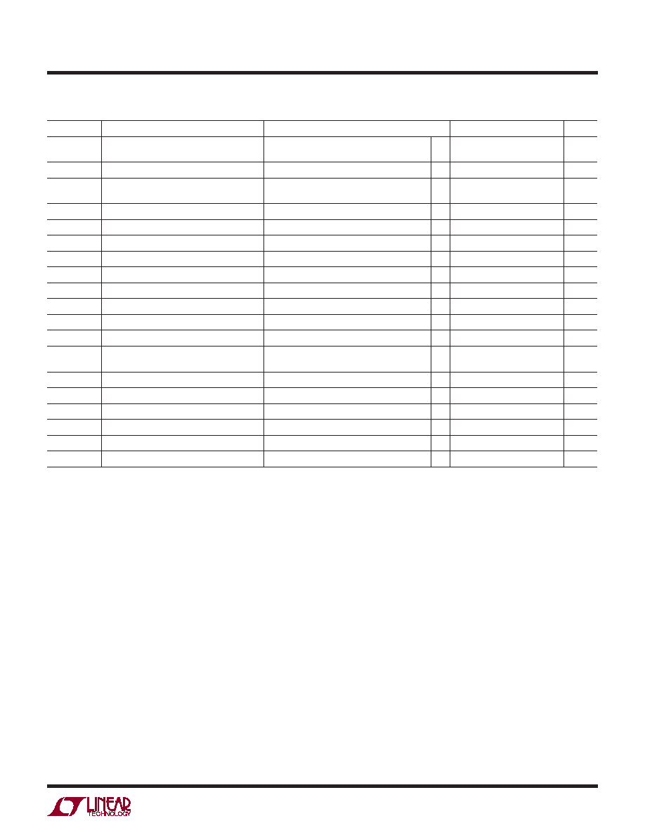
TIMING CHARACTERISTICS The l denotes the specications which apply over the full operating temperature
range, otherwise specications are at TA = 25°C. (Note 5)
SYMBOL
PARAMETER
CONDITIONS
MIN
TYP
MAX
UNITS
fSAMPLE(MAX)
Maximum Sampling Frequency
Through CH0 to CH7 Inputs
Through ADC+, ADC– Only
l
100
166
kHz
tCONV
Conversion Time
l
45
μs
tACQ
Acquisition Time
Through CH0 to CH7 Inputs
Through ADC+, ADC– Only
l
1
4μs
μs
fSCK
SCK Frequency
(Note 14)
l
020
MHz
tr
SDO Rise Time
See Test Circuits
6
ns
tf
SDO Fall Time
See Test Circuits
6
ns
t1
CONVST High Time
l
40
ns
t2
CONVST to BUSY Delay
CL = 25pF, See Test Circuits
l
15
30
ns
t3
SCK Period
l
50
ns
t4
SCK High
l
10
ns
t5
SCK Low
l
10
ns
t6
Delay Time, SCK
↓ to SDO Valid
CL = 25pF, See Test Circuits
l
25
45
ns
t7
Time from Previous SDO Data Remains
Valid After SCK
↓
CL = 25pF, See Test Circuits
l
520
ns
t8
SDO Valid After RD
↓
CL = 25pF, See Test Circuits
l
11
30
ns
t9
RD↓ to SCK Setup Time
l
20
ns
t10
SDI Setup Time Before SCK
↑
l
0ns
t11
SDI Hold Time After SCK
↑
l
7ns
t12
SDO Valid Before BUSY
↑
RD = Low, CL = 25pF, See Test Circuits
l
520
ns
t13
Bus Relinquish Time
See Test Circuits
l
10
30
ns
Note 1: Stresses beyond those listed under Absolute Maximum Ratings
may cause permanent damage to the device. Exposure to any Absolute
Maximum Rating condition for extended periods may affect device
reliability and lifetime.
Note 2: All voltage values are with respect to ground with DGND, AGND1,
AGND2 and AGND3 wired together unless otherwise noted.
Note 3: When these pin voltages are taken below ground or above AVDD =
DVDD = OVDD = VDD, they will be clamped by internal diodes. This product
can handle currents of greater than 100mA below ground or above VDD
without latchup.
Note 4: When these pin voltages are taken below ground they will be
clamped by internal diodes. This product can handle currents of greater
than 100mA below ground without latchup. These pins are not clamped
to VDD.
Note 5: VDD = 5V, fSAMPLE = 100kHz, tr = tf = 5ns unless otherwise
specied.
Note 6: Linearity, offset and full-scale specications apply for a single-
ended analog MUX input with respect to ground or ADC+ with respect to
ADC– tied to ground.
Note 7: Integral nonlinearity is dened as the deviation of a code from a
straight line passing through the actual end points of the transfer curve.
The deviation is measured from the center of the quantization band.
Note 8: Bipolar zero error is the offset voltage measured from – 0.5LSB
when the output code ickers between 0000 0000 0000 0000 and 1111
1111 1111 1111 for the LTC1859, between 00 0000 0000 0000 and 11
1111 1111 1111 for the LTC1858 and between 0000 0000 0000 and
1111 1111 1111 for the LTC1857. Unipolar zero error is the offset voltage
measured from 0.5LSB when the output codes icker between 0000 0000
0000 0000 and 0000 0000 0000 0001 for the LTC1859, between 00 0000
0000 0000 and 00 0000 0000 0001 for the LTC1858 and between 0000
0000 0000 and 0000 0000 0001 for the LTC1857.
Note 9: Guaranteed by design, not subject to test.
Note 10: Recommended operating conditions.
Note 11: Full-scale bipolar error is the worst case of –FS or +FS
untrimmed deviation from ideal rst and last code transitions, divided by
the full-scale range, and includes the effect of offset error. For unipolar
full-scale error, the deviation of the last code transition from ideal, divided
by the full-scale range, and includes the effect of offset error.
Note 12: All Specications in dB are referred to a full-scale ±10V input.
Note 13: Recovers to specied performance after (2 FS) input
overvoltage.
Note 14: t6 of 45ns maximum allows fSCK up to 10MHz for rising capture
with 50% duty cycle and fSCK up to 20MHz for falling capture (with 5ns
setup time for the receiving logic).
Note 15: The specication is referred to the ±10V input range.
相关PDF资料 |
PDF描述 |
|---|---|
| EBM12DTBT-S189 | CONN EDGECARD 24POS R/A .156 SLD |
| GBA14DRST-S288 | CONN EDGECARD 28POS .125 EXTEND |
| EBM12DTAT-S189 | CONN EDGECARD 24POS R/A .156 SLD |
| SLP681M100A1P3 | CAP ALUM 680UF 100V 20% SNAP |
| RBM11DSEI-S13 | CONN EDGECARD 22POS .156 EXTEND |
相关代理商/技术参数 |
参数描述 |
|---|---|
| DC684A | 制造商:Linear Technology 功能描述:DEMO BOARD FOR LT4256-3 制造商:Linear Technology 功能描述:EVAL BOARD, LT4256-3GN HOT SWAP CONTR |
| DC-697ZTZ | 制造商:Texas Instruments 功能描述: |
| DC6M401X6/285S,135 | 制造商:NXP Semiconductors 功能描述:DC6M401X6/NONE/REELLG//285S - Tape and Reel 制造商:NXP Semiconductors 功能描述:IC REG BUCK 2.85V 425MA 6-WLCSP |
| DC6M401X6-18S | 制造商:PHILIPS 制造商全称:NXP Semiconductors 功能描述:Small, highly efficient switching converters |
| DC6M401X6-285S | 制造商:PHILIPS 制造商全称:NXP Semiconductors 功能描述:Small, highly efficient switching converters |
发布紧急采购,3分钟左右您将得到回复。