- 您现在的位置:买卖IC网 > PDF目录17065 > DC941A (Linear Technology)BOARD DELTA SIGMA ADC LTC2482 PDF资料下载
参数资料
| 型号: | DC941A |
| 厂商: | Linear Technology |
| 文件页数: | 11/32页 |
| 文件大小: | 0K |
| 描述: | BOARD DELTA SIGMA ADC LTC2482 |
| 软件下载: | QuikEval System |
| 设计资源: | DC941A Design File DC941A Schematic |
| 标准包装: | 1 |
| 系列: | Easy Drive™, QuikEval™ |
| ADC 的数量: | 1 |
| 位数: | 16 |
| 采样率(每秒): | 6.8 |
| 数据接口: | MICROWIRE?,串行,SPI? |
| 工作温度: | 0°C ~ 70°C |
| 已用 IC / 零件: | LTC2482 |
| 已供物品: | 板 |
| 相关产品: | LTC2482IDD#TRPBF-ND - IC ADC 16BIT 10-DFN LTC2482CDD#TRPBF-ND - IC ADC 16BIT 10-DFN LTC2482IDD#PBF-ND - IC ADC 16BIT 10-DFN LTC2482CDD#PBF-ND - IC ADC 16BIT 10-DFN |
第1页第2页第3页第4页第5页第6页第7页第8页第9页第10页当前第11页第12页第13页第14页第15页第16页第17页第18页第19页第20页第21页第22页第23页第24页第25页第26页第27页第28页第29页第30页第31页第32页
LTC2482
19
2482fc
APPLICATIONS INFORMATION
A similar situation may occur during the sleep state when
CS is pulsed high-low-high in order to test the conversion
status. If the device is in the sleep state (EOC = 0), SCK
will go low. Once CS goes high (within the time period
dened above as tEOCtest), the internal pull-up is activated.
For a heavy capacitive load on the SCK pin, the internal
pull-up may not be adequate to return SCK to a high level
before CS goes low again. This is not a concern under
normal conditions where CS remains low after detecting
EOC = 0. This situation is easily overcome by adding an
external 10k pull-up resistor to the SCK pin.
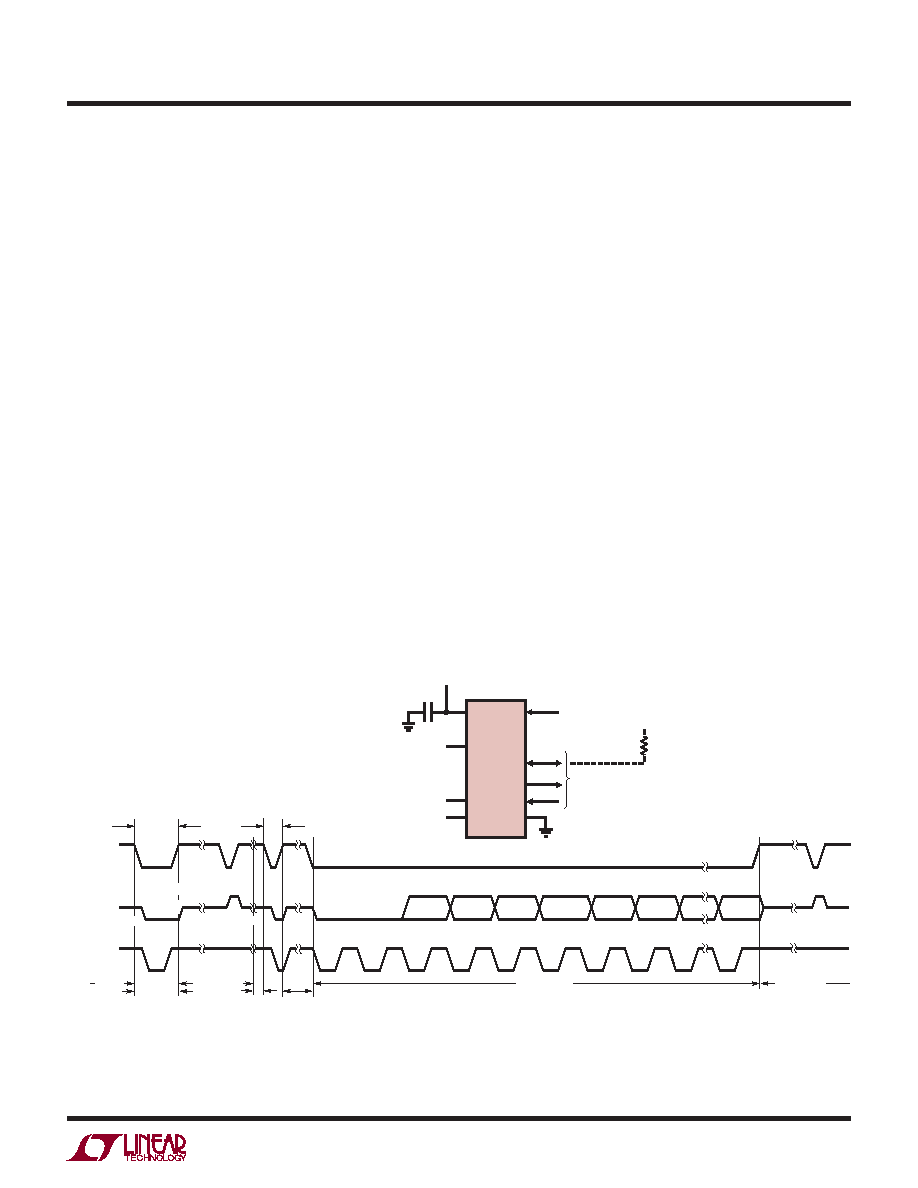
Internal Serial Clock, 2-Wire I/O,
Continuous Conversion
This timing mode uses a 2-wire (output only) interface.
The conversion result is shifted out of the device by an
internally generated serial clock (SCK) signal (see Figure 9).
CSmaybepermanentlytiedtoground,simplifyingtheuser
interface or transmission over an isolation barrier.
The internal serial clock mode is selected at the end of the
power-on reset (POR) cycle. The POR cycle is concluded
approximately 1ms after VCC exceeds 2V. An internal weak
pull-up is active during the POR cycle; therefore, the internal
serial clock timing mode is automatically selected if SCK
is not externally driven low (if SCK is loaded such that the
internal pull-up cannot pull the pin high, the external SCK
mode will be selected).
During the conversion, the SCK and the serial data output
pin (SDO) are high (EOC = 1). Once the conversion is
complete, SCK and SDO go low (EOC = 0) indicating the
conversion has nished and the device has entered the low
power sleep state. The part remains in the sleep state a
minimum amount of time (1/2 the internal SCK period) then
immediately begins outputting data. The data input/output
cycle begins on the rst rising edge of SCK and ends after
the 24th rising edge. The output data is shifted out of the
SDO pin on each falling edge of SCK. The internally gener-
ated serial clock is output to the SCK pin. This signal may
be used to shift the conversion result into external circuitry.
EOC can be latched on the rst rising edge of SCK and the
last bit of the conversion result can be latched on the 24th
rising edge of SCK. After the 24th rising edge, SDO goes
high (EOC = 1) indicating a new conversion is in progress.
SCK remains high during the conversion.
SDO
SCK
(INTERNAL)
CS
>tEOCtest
MSB
SIG
BIT 8
TEST EOC
(OPTIONAL)
TEST EOC
BIT 19
BIT 18
BIT 17
BIT 16
BIT 20
BIT 21
BIT 22
EOC
BIT 23
EOC
BIT 0
SLEEP
DATA OUTPUT
Hi-Z
DATA
OUTPUT
CONVERSION
SLEEP
2482 F08
<tEOCtest
TEST EOC
VCC
fO
VREF
IN+
IN–
SCK
SDO
CS
GND
210
INT/EXT CLOCK
3
4
5
9
10k
VCC
7
8,1
6
REFERENCE
VOLTAGE
0.1V TO VCC
ANALOG
INPUT
1μF
2.7V TO 5.5V
LTC2482
3-WIRE
SPI INTERFACE
Hi-Z
Figure 8. Internal Serial Clock, Reduce Data Output Length
相关PDF资料 |
PDF描述 |
|---|---|
| SDR0604-102KL | INDUCTOR POWER 1000UH 10% SMD |
| AD9750-EBZ | BOARD EVAL FOR AD9750 |
| LGU2W820MELA | CAP ALUM 82UF 450V 20% SNAP |
| AD9752-EBZ | BOARD EVAL FOR AD9752 |
| AD9754-EBZ | BOARD EVAL FOR AD9754 |
相关代理商/技术参数 |
参数描述 |
|---|---|
| DC945KB | 制造商:DEWALT 功能描述:DRILL KIT CORDLESS 12V |
| DC945KB-GB | 制造商:DEWALT 功能描述:DRILL 12V |
| DC-9-500-2.1P | 制造商:SR COMPONENTS 功能描述: 制造商:SR Components Inc 功能描述: |
| DC-9-500-3.5P | 制造商:SR COMPONENTS 功能描述: 制造商:SR Components Inc 功能描述: |
| DC950KX | 制造商:Dewalt 功能描述:18V Hammer Drill/Driver with 1/2" Chuck |
发布紧急采购,3分钟左右您将得到回复。