- 您现在的位置:买卖IC网 > Datasheet目录320 > DK-DEV-5M570ZN (Altera)KIT DEV MAX V 5M570Z Datasheet资料下载
参数资料
| 型号: | DK-DEV-5M570ZN |
| 厂商: | Altera |
| 文件页数: | 10/30页 |
| 文件大小: | 0K |
| 描述: | KIT DEV MAX V 5M570Z |
| 产品培训模块: | Max V Overview Three Reasons to Use FPGA's in Industrial Designs |
| 特色产品: | Max V CPLD Development Kit |
| 标准包装: | 1 |
| 系列: | MAX® V |
| 类型: | CPLD |
| 适用于相关产品: | 5M570ZF256 |
| 所含物品: | 板,线缆,软件和文档 |
| 相关产品: | 5M570ZF256I5N-ND - IC MAX V CPLD 570 LE 256-FBGA 5M570ZF256C4N-ND - IC MAX V CPLD 570 LE 256-FBGA 544-2721-ND - IC MAX V CPLD 570 LE 256-FBGA |
| 其它名称: | 544-2722 |
第1页第2页第3页第4页第5页第6页第7页第8页第9页当前第10页第11页第12页第13页第14页第15页第16页第17页第18页第19页第20页第21页第22页第23页第24页第25页第26页第27页第28页第29页第30页
�� �
�
�3–10�
�Chapter� 3:� DC� and� Switching� Characteristics� for� MAX� V� Devices�
�Power� Consumption�
�Power� Consumption�
�You� can� use� the� Altera� ?� PowerPlay� Early� Power� Estimator� and� PowerPlay� Power�
�Analyzer� to� estimate� the� device� power.�
���in� volume� 3� of� the� Quartus� II� Handbook.�
�Timing� Model� and� Specifications�
�MAX� V� devices� timing� can� be� analyzed� with� the� Altera� Quartus� ?� II� software,� a� variety�
�of� industry-standard� EDA� simulators� and� timing� analyzers,� or� with� the� timing� model�
��MAX� V� devices� have� predictable� internal� delays� that� allow� you� to� determine� the�
�worst-case� timing� of� any� design.� The� software� provides� timing� simulation,�
�point-to-point� delay� prediction,� and� detailed� timing� analysis� for� device-wide�
�performance� evaluation.�
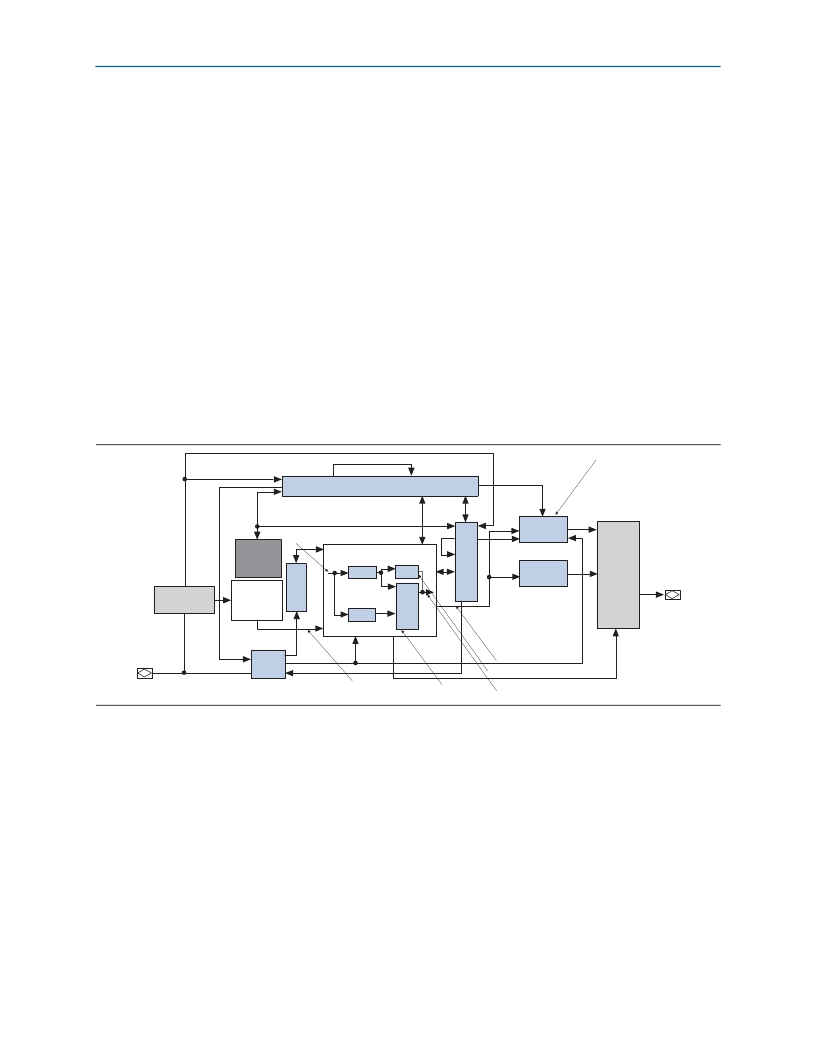
�Figure� 3–2.� Timing� Model� for� MAX� V� Devices�
�Output� and� Output� Enable�
�Data� Delay�
�t� R4�
�t� IODR�
�Data-I� n� /LUT� Chai� n�
�t� IOE�
�t� SU�
�t� H�
�I/O Input Delay�
�t� IN�
�User�
�Flash�
�Memory�
�Input� Routing�
�Delay�
�t� DL�
�Logic� Element�
�LUT� Delay�
�t� LUT� t� COMB�
�t� CO�
�Register� Control�
�Delay�
�t� C� t� PRE�
�t� CLR�
�t� C4�
�Output� Routing�
�Delay�
�t� FASTIO�
�Output�
�Delay�
�t� OD�
�t� XZ�
�t� ZX�
�I/O� Pin�
�I/O� Pin�
�INPUT�
�t� GLOB�
�F� r� om� Adjace� n� t� LE�
�Combi� n� atio� n� al� Path� Delay�
�Global� Input� Delay�
�To� Adjace� n� t� LE�
�Regi� s� te� r� Delay� s�
�Data-O� u� t�
�You� can� derive� the� timing� characteristics� of� any� signal� path� from� the� timing� model�
�and� parameters� of� a� particular� device.� You� can� calculate� external� timing� parameters,�
�which� represent� pin-to-pin� timing� delays,� as� the� sum� of� the� internal� parameters.�
���May� 2011�
�Altera� Corporation�
�相关PDF资料 |
PDF描述 |
|---|---|
| DK-DEV-5SGXEA7N | KIT DEV STRATIX V FPGA 5SGXEA7 |
| DK-DSP-2S180N | DSP PRO KIT W/SII EP2S180N |
| DK-DSP-3C120N | KIT DEV DSP CYCLONE III EDITION |
| DK-K7-CONN-CES-G | KINTEX-7 FPGA CONNECTIVITY KIT |
| DK-K7-EMBD-CES-G-J | KINTEX-7 FPGA EMBEDDED KIT JAPAN |
相关代理商/技术参数 |
参数描述 |
|---|---|
| DK-DEV-5SGSMD5N | 功能描述:可编程逻辑 IC 开发工具 FPGA Development Kit For 5SGSMD5K2 RoHS:否 制造商:Altera Corporation 产品:Development Kits 类型:FPGA 工具用于评估:5CEFA7F3 接口类型: 工作电源电压: |
| DK-DEV-5SGSMD5N/P | 制造商:Altera Corporation 功能描述:DSP DEVELOPMENT KIT,STRATIX V |
| DK-DEV-5SGXEA7/ES | 功能描述:可编程逻辑 IC 开发工具 FPGA Development Kit For 5SGXEA7 ES RoHS:否 制造商:Altera Corporation 产品:Development Kits 类型:FPGA 工具用于评估:5CEFA7F3 接口类型: 工作电源电压: |
| DK-DEV-5SGXEA7N | 功能描述:可编程逻辑 IC 开发工具 FPGA Development Kit For 5SGXEA7K2F40C2N RoHS:否 制造商:Altera Corporation 产品:Development Kits 类型:FPGA 工具用于评估:5CEFA7F3 接口类型: 工作电源电压: |
| DK-DSP-2C70N | 功能描述:DSP KIT W/CYCLONE II EPS2C70N RoHS:是 类别:编程器,开发系统 >> 通用嵌入式开发板和套件(MCU、DSP、FPGA、CPLD等) 系列:Cyclone® II 产品培训模块:Blackfin® Processor Core Architecture Overview Blackfin® Device Drivers Blackfin® Optimizations for Performance and Power Consumption Blackfin® System Services 特色产品:Blackfin? BF50x Series Processors 标准包装:1 系列:Blackfin® 类型:DSP 适用于相关产品:ADSP-BF548 所含物品:板,软件,4x4 键盘,光学拨轮,QVGA 触摸屏 LCD 和 40G 硬盘 配用:ADZS-BFBLUET-EZEXT-ND - EZ-EXTENDER DAUGHTERBOARDADZS-BFLLCD-EZEXT-ND - BOARD EXT LANDSCAP LCD INTERFACE 相关产品:ADSP-BF542BBCZ-4A-ND - IC DSP 16BIT 400MHZ 400CSBGAADSP-BF544MBBCZ-5M-ND - IC DSP 16BIT 533MHZ MDDR 400CBGAADSP-BF542MBBCZ-5M-ND - IC DSP 16BIT 533MHZ MDDR 400CBGAADSP-BF542KBCZ-6A-ND - IC DSP 16BIT 600MHZ 400CSBGAADSP-BF547MBBCZ-5M-ND - IC DSP 16BIT 533MHZ MDDR 400CBGAADSP-BF548BBCZ-5A-ND - IC DSP 16BIT 533MHZ 400CSBGAADSP-BF547BBCZ-5A-ND - IC DSP 16BIT 533MHZ 400CSBGAADSP-BF544BBCZ-5A-ND - IC DSP 16BIT 533MHZ 400CSBGAADSP-BF542BBCZ-5A-ND - IC DSP 16BIT 533MHZ 400CSBGA |
发布紧急采购,3分钟左右您将得到回复。