参数资料
| 型号: | DLP-HS-FPGA3 |
| 厂商: | DLP Design Inc |
| 文件页数: | 2/18页 |
| 文件大小: | 0K |
| 描述: | MODULE USB-TO-FPGA SPARTAN 3A |
| 标准包装: | 1 |
| 系列: | FPGA |
| 模块/板类型: | FPGA 模块 |
| 适用于相关产品: | USB |
| 其它名称: | 813-1036 |
Rev. 1.1 (April 2012)
10
DLP Design, Inc.
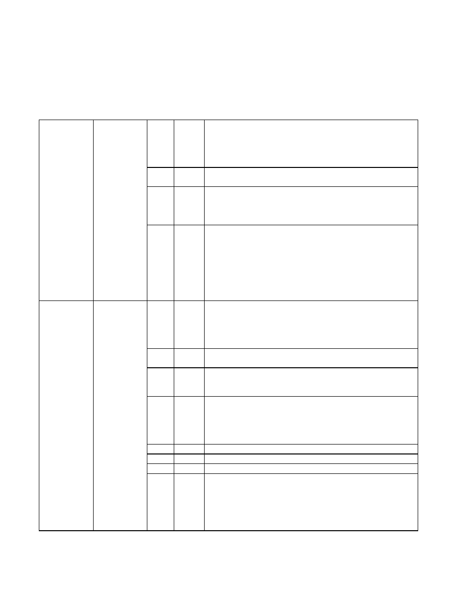
For example, a write to a column starting address of 0 will write to column locations 0, 1, 2 and 3. But
if the user then writes to column address 1, they will actually be writing to column locations 1, 2, 3 and
0, which will overwrite the previous write operation.
More details on how the DDR2 SDRAM column bits 1 and 0 function can be found in Figure 4 and
Table 40 of the Micron MT47H32M8 datasheet. For details on how the bank, row and column bits
are sent via USB to the memory, refer to the commands below:
Memory
Read
Reads 4
bytes from
the DDR2
SDRAM
0
0x8n
Reads 4 bytes from the DDR2 SDRAM starting with the
address specified. The command byte is OR’d with the
Most Significant Row Address Bit (24).
n = 0 the Most Sig Row Address Bit is low (0x80)
n = 1 the Most Sig Row Address Bit is high (0x81)
1
0xah
Bits 23-16: Middle 8 bits of Row Address to be read
from
2
0xam
Bits 15-12: Lower 4 bits of Row Address to be read
from
Bits 11-8: Upper 4 bits of Column Address to be read
from
3
0xal
Bits 7-2: Lower 6 bits of Column Address to be read
from
NOTES: Refer to the text above regarding Column Bits
1 and 0 (equates to 0xal bits 3-2). Bits 1-0: Bank
Address to be read from. If the memory has not been
initialized, the data returned will be invalid, and the
command returned will be 0xE7 indicating the error.
Memory
Write
Writes 4
bytes to the
DDR2
SDRAM
0
0x9n
Writes 4 bytes to the DDR2 SDRAM starting with the
address specified. The command byte is OR’d with the
Most Significant Row Address bit (24).
n = 0 the Most Sig Row Address Bit is low (0x90)
n = 1 the Most Sig Row Address Bit is high (0x91)
1
0xah
Bits 23-16: Middle 8 bits of Row Address to be written
to
2
0xam
Bits 15-12: Lower 4 bits of Row Address to be written to
Bits 11-8: Upper 4 bits of Column Address to be written
to
3
0xal
Bits 7-2: Lower 6 bits of column address to be written to
NOTE: Refer to the text above regarding Column Bits 1
and 0 (equates to 0xal bits 3-2). Bits 1-0: Bank
Address to be written to
4
0xd0
Data Byte 0 written to Address Specified
5
0xd1
Data Byte 1 written to Address Specified + 1
6
0xd2
Data Byte 2 written to Address Specified + 2
7
0xd3
Data Byte 3 written to Address Specified + 3. Returns
the 4 bytes written followed by an echo back of the
command and address data sent.
NOTE: If the memory has not been initialized, the
command returned will be 0xE7 indicating the error.
相关PDF资料 |
PDF描述 |
|---|---|
| DP83848CVVX/NOPB | TXRX ETHERNET PHYTER 48LQFP |
| DP83848HSQ/NOPB | IC TXRX ETHERNET PHYTER 40-LLP |
| DP83848YB/NOPB | IC TXRX ETHERNET PHYTERA 48-LQFP |
| DRM4000-N00-232 | DRM 4000 MODULE |
| DRM4000L-N00-232 | MODULE DEAD RECKONING RS-232 |
相关代理商/技术参数 |
参数描述 |
|---|---|
| DLP-HS-FPGA-A | 功能描述:FPGA Embedded Module Spartan-3A, XC3S200A FT2232H 66MHz 32MB 制造商:dlp design inc. 系列:FPGA 零件状态:有效 模块/板类型:FPGA,USB ?? 核心处理器:Spartan-3A,XC3S200A 协处理器:FT2232H 速度:66MHz 闪存大小:- RAM 容量:32Mb 连接器类型:USB - B,引脚接头 大小/尺寸:3" x 1.2"(76.2mm x 30.5mm) 工作温度:0°C ~ 70°C 标准包装:1 |
| DLP-IO14 | 功能描述:数据记录与采集 14-Channel Data-Acq Module RoHS:否 制造商:Lantronix 描述/功能:Analog device server 显示器类型:None 电流额定值: |
| DLP-IO16 | 功能描述:界面模块 USB/Micro Dev Board RoHS:否 制造商:4D Systems 产品:Serial Converters 通道/端口数量: 数据速率: 接口类型:USB, UART 工作电源电压:3.3 V, 5 V 最大工作温度: |
| DLP-IO20 | 功能描述:数据记录与采集 USB-BASED 20-CHANNEL DATA ACQUISITION MOD RoHS:否 制造商:Lantronix 描述/功能:Analog device server 显示器类型:None 电流额定值: |
| DLP-IO26 | 功能描述:开发板和工具包 - PIC / DSPIC USB/Micro Dev Board RoHS:否 制造商:Microchip Technology 产品:Starter Kits 工具用于评估:chipKIT 核心:Uno32 接口类型: 工作电源电压: |
发布紧急采购,3分钟左右您将得到回复。