- 您现在的位置:买卖IC网 > PDF目录21914 > DMN3029LFG-13 (Diodes Inc)MOSFET N-CH 30V 5.3A PWRDI333-8 PDF资料下载
参数资料
| 型号: | DMN3029LFG-13 |
| 厂商: | Diodes Inc |
| 文件页数: | 2/7页 |
| 文件大小: | 0K |
| 描述: | MOSFET N-CH 30V 5.3A PWRDI333-8 |
| 标准包装: | 1 |
| FET 型: | MOSFET N 通道,金属氧化物 |
| FET 特点: | 逻辑电平门 |
| 漏极至源极电压(Vdss): | 30V |
| 电流 - 连续漏极(Id) @ 25° C: | 5.3A |
| 开态Rds(最大)@ Id, Vgs @ 25° C: | 18.6 毫欧 @ 10A,10V |
| Id 时的 Vgs(th)(最大): | 1.8V @ 250µA |
| 闸电荷(Qg) @ Vgs: | 11.3nC @ 10V |
| 输入电容 (Ciss) @ Vds: | 580pF @ 15V |
| 功率 - 最大: | 1W |
| 安装类型: | 表面贴装 |
| 封装/外壳: | 8-PowerVDFN |
| 供应商设备封装: | PowerDI3333-8 |
| 包装: | 标准包装 |
| 其它名称: | DMN3029LFG-13DIDKR |
�� �
�
�DMN3029LFG�
�Maximum� Ratings� (@T� A� =� +25°C,� unless� otherwise� specified.)�
�Drain-Source� Voltage�
�Gate-Source� Voltage�
�Characteristic�
�Symbol�
�V� DSS�
�V� GSS�
�Value�
�30�
�±25�
�Unit�
�V�
�V�
�Continuous� Drain� Current� (Note� 5)� V� GS� =� 10V�
�Continuous� Drain� Current� (Note� 6)� V� GS� =� 10V�
�Continuous� Drain� Current� (Note� 6)� V� GS� =� 10V�
�Continuous� Drain� Current� (Note� 6)� V� GS� =� 4.5V�
�Continuous� Drain� Current� (Note� 6)� V� GS� =� 4.5V�
�Steady�
�State�
�Steady�
�State�
�t� ≤� 10s�
�Steady�
�State�
�t� ≤� 10s�
�T� A� =� +25°C�
�T� A� =� +70°C�
�T� A� =� +25°C�
�T� A� =� +70°C�
�T� A� =� +25°C�
�T� A� =� +70°C�
�T� A� =� +25°C�
�T� A� =� +70°C�
�T� A� =� +25°C�
�T� A� =� +70°C�
�I� D�
�I� D�
�I� D�
�I� D�
�I� D�
�5.3�
�4.2�
�8.0�
�6.3�
�9.5�
�7.7�
�6.5�
�4.9�
�7.8�
�6.2�
�A�
�A�
�A�
�A�
�A�
�Pulsed� Drain� Current� (Note� 7)�
�Avalanche� Current� (Notes� 7� &� 8)�
�Repetitive� Avalanche� Energy� (Notes� 7� &� 8)� L� =� 0.1mH�
�I� DM�
�I� AR�
�E� AR�
�70�
�18�
�16�
�A�
�A�
�mJ�
�Thermal� Characteristics�
�Characteristic�
�Power� Dissipation� (Note� 5)�
�Thermal� Resistance,� Junction� to� Ambient� @T� A� =� +25°C� (Note� 5)�
�Power� Dissipation� (Note� 6)�
�Thermal� Resistance,� Junction� to� Ambient� @T� A� =� +25°C� (Note� 6)�
�Power� Dissipation� (Note� 6)� t� ≤� 10s�
�Thermal� Resistance,� Junction� to� Ambient� @T� A� =� +25°C� (Note� 6)� t� ≤� 10s�
�Operating� and� Storage� Temperature� Range�
�Notes:�
�5.� Device� mounted� on� FR-4� PCB� with� minimum� recommended� pad� layout,� single� sided.�
�Symbol�
�P� D�
�R� θ� JA�
�P� D�
�R� θ� JA�
�P� D�
�R� θ� JA�
�T� J� ,� T� STG�
�Max�
�1.0�
�130.6�
�2.07�
�62.5�
�3.0�
�43.8�
�-55� to� +150�
�Unit�
�W�
�°C/W�
�W�
�°C/W�
�W�
�°C/W�
�°C�
�6.� Device� mounted� on� 2”� x� 2”� FR-4� PCB� with� high� coverage� 2� oz.� Copper,� single� sided.�
�7.� Repetitive� rating,� pulse� width� limited� by� junction� temperature.�
�8.� I� AR� and� E� AR� rating� are� based� on� low� frequency� and� duty� cycles� to� keep� T� J� =� +25°C.�
�100�
�R� DS(on)�
�P� W� = 10μ s�
�400�
�10�
�Limited�
�DC�
�350�
�300�
�250�
�Single� Pulse�
�R� θ� JA� =� 60� °� C/W�
�R� θ� JA(t)� =� r� (t)� *� R� θ� JA�
�T� J� -� T� A� =� P� *� R� θ� JA(t)�
�1�
�0.1�
�P� W� = 10s�
�P� W� = 1s�
�P� W� = 100ms�
�P� W� = 10ms�
�P� W� = 1ms�
�P� W� = 100μs�
�T� J(max)� =� 150°C�
�T� A� =� 25°C�
�Single� Pulse�
�200�
�150�
�100�
�50�
�0.01�
�0.1�
�1�
�10�
�100�
�0�
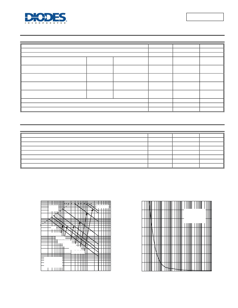
�0.0001� 0.001� 0.01� 0.1� 1� 10� 100� 1,000�
�V� DS� ,� DRAIN-SOURCE� VOLTAGE� (V)�
�Fig.� 1� SOA,� Safe� Operation� Area�
�POWERDI� is� a� registered� trademark� of� Diodes� Incorporated.�
�t1,� PULSE� DURATION� TIME� (sec)�
�Fig.� 2� Single� Pulse� Maximum� Power� Dissipation�
�DMN3029LFG�
�Document� number:� DS35448� Rev.� 7� -� 2�
�2� of� 7�
�www.diodes.com�
�October� 2012�
�?� Diodes� Incorporated�
�相关PDF资料 |
PDF描述 |
|---|---|
| 2239-C-48 | MULTI-STACK BANANA PLUG RG58 48" |
| A1186LLHLT-T | IC SWITCH HALL EFFECT UNI SOT-23 |
| A1186EUA-T | IC SWITCH HALL EFFECT UNI 3-SIP |
| A1186ELHLT-T | IC SWITCH HALL EFFECT UNI SOT-23 |
| 1368-A-30 | DBL BANA PLUG/BANA BREAKOUT 30" |
相关代理商/技术参数 |
参数描述 |
|---|---|
| DMN3029LFG-7 | 功能描述:MOSFET N-CH 30V 5.3A PWRDI333-8 RoHS:是 类别:分离式半导体产品 >> FET - 单 系列:- 标准包装:1,000 系列:MESH OVERLAY™ FET 型:MOSFET N 通道,金属氧化物 FET 特点:逻辑电平门 漏极至源极电压(Vdss):200V 电流 - 连续漏极(Id) @ 25° C:18A 开态Rds(最大)@ Id, Vgs @ 25° C:180 毫欧 @ 9A,10V Id 时的 Vgs(th)(最大):4V @ 250µA 闸电荷(Qg) @ Vgs:72nC @ 10V 输入电容 (Ciss) @ Vds:1560pF @ 25V 功率 - 最大:40W 安装类型:通孔 封装/外壳:TO-220-3 整包 供应商设备封装:TO-220FP 包装:管件 |
| DMN3030LFG-7 | 功能描述:MOSFET 650V N-Ch Enh FET 30V VDSS 25V VGSS RoHS:否 制造商:STMicroelectronics 晶体管极性:N-Channel 汲极/源极击穿电压:650 V 闸/源击穿电压:25 V 漏极连续电流:130 A 电阻汲极/源极 RDS(导通):0.014 Ohms 配置:Single 最大工作温度: 安装风格:Through Hole 封装 / 箱体:Max247 封装:Tube |
| DMN3030LSS | 制造商:DIODES 制造商全称:Diodes Incorporated 功能描述:SINGLE N-CHANNEL ENHANCEMENT MODE MOSFET |
| DMN3030LSS-13 | 功能描述:MOSFET NMOS SINGLE N-CHANNL 30V 9A RoHS:否 制造商:STMicroelectronics 晶体管极性:N-Channel 汲极/源极击穿电压:650 V 闸/源击穿电压:25 V 漏极连续电流:130 A 电阻汲极/源极 RDS(导通):0.014 Ohms 配置:Single 最大工作温度: 安装风格:Through Hole 封装 / 箱体:Max247 封装:Tube |
| DMN3031LSS | 制造商:DIODES 制造商全称:Diodes Incorporated 功能描述:SINGLE N-CHANNEL ENHANCEMENT MODE MOSFET |
发布紧急采购,3分钟左右您将得到回复。