- 您现在的位置:买卖IC网 > PDF目录295503 > DS-11802D4-464Y (DATA DEVICE CORP) DIGITAL TO SYNCHRO OR RESOLVER, CDIP28 PDF资料下载
参数资料
| 型号: | DS-11802D4-464Y |
| 厂商: | DATA DEVICE CORP |
| 元件分类: | 位置变换器 |
| 英文描述: | DIGITAL TO SYNCHRO OR RESOLVER, CDIP28 |
| 封装: | CERAMIC, DDIP-28 |
| 文件页数: | 4/8页 |
| 文件大小: | 341K |
| 代理商: | DS-11802D4-464Y |
DIGITAL-TO-RESOLVER/SYNCHRO CONVERTERS
The output of the DS-11802 is a single-ended sin/cos.
FIGURE 8 illustrates a schematic for a 4-Wire Digital-to-Resolver
Converter (S1, S2, S3, and S4) using external power amplifiers
and transformers.
FIGURE 9 illustrates a schematic for 3-Wire Digital-to-Synchro
Converter (S1, S2, and S3) using an additional power stage and
external transformers.
A benefit to the designs shown in FIGURES 8 and 9 is the abili-
ty to keep the converters near the digital data and control sig-
nals, and to mount the power amplifiers and transformers in a
better thermal location. This would isolate heat dissipating cir-
cuits from high-accuracy computing circuits.
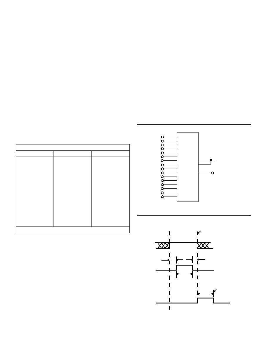
1. The LDC is low (logic 0) so that the contents of the holding reg-
ister are latched and will remain unaffected by the changes on
the input registers.
2. When the LBE is set high (logic 1) the 8 LSBs (B9-B16) are
transferred to the low byte. The LBE must remain high for a min-
imum of 800 nsec after the data is stable. The data should
remain stable for 200 nsec after the LBE is set low (logic 0).
3. When the HBE is set high (logic 1) the 8 MSBs (B1-B8) are
transferred to the low byte. The HBE must remain high for a min-
imum of 800 nsec after the data is stable. The data should
remain stable for 200 nsec after the HBE is set low (logic 0).
4. When the LDC is set high (logic 1) the data is transferred from
the two input registers to the holding register. The LDC should
be held high for 600 nsec minimum. Once the LDC is set low,
the cycle can begin again.
Note: LBE, HBE, and LDC are level-actuated functions. Refer to
TABLE 3 for bit values.
4
B1
B2
B3
B4
B5
B6
B13
B12
B11
B10
B9
B8
B7
B14
B15
B16
(LSB)
(MSB)
1
2
3
4
5
6
7
8
11
12
13
14
15
16
17
18
DS-11802
LBE
HBE
LDC
LOAD
CONVERTER
NOT CONNECTED
OR LOAD DATA PULSE
10
9
19
FIGURE 6. DATA TRANSFER FROM 16-BIT BUS
600 ns
MIN
DATA TRANSFERRED TO
HOLDING REGISTERS
DATA
CHANGING
DATA
STEADY
ALL 16 BITS
DATA TRANSFERRED
TO INPUT REGISTERS
DATA
HBE LBE
LDC
200 ns
MIN
200 ns
MIN
800 ns
MIN
FIGURE 7. TIMING FOR 16-BIT BUS TRANSFER
Note:
HBE enables the MSBs and LBE enables the LSBs.
10800.0
5400.0
2700.0
1350.0
675.0
337.5
168.75
84.38
42.19
21.09
10.55
5.27
2.64
1.32
0.66
0.33
180.0
90.0
45.0
22.5
11.25
5.625
2.813
1.406
0.7031
0.3516
0.1758
0.0879
0.0439
0.0220
0.0110
0.0055
1 MSB
2
3
4
5
6
7
8
9
10
11
12
13
14
15
16
MIN/BIT
DEG/BIT
BIT
TABLE 3. DIGITAL ANGLE INPUTS
DATA TRANSFER FROM A 16-BIT DATA BUS
Applications interfacing with a 16-bit data bus require only single
byte loading (see FIGURE 6). LBE and HBE are either uncon-
nected or tied together and pulsed high to load data.
As shown in the timing diagram (see FIGURE 7) 200 nsec after
the data has been stable, the LDC is set high (logic 1) to trans-
fer the data to the holding register. Since LDC is level actuated,
it must remain high for the time specified (600 nsec).
相关PDF资料 |
PDF描述 |
|---|---|
| DS1075M-60 | 60 MHz, OTHER CLOCK GENERATOR, PDIP8 |
| DS1233Z-10N | 1-CHANNEL POWER SUPPLY SUPPORT CKT, PDSO4 |
| DS1283SN | 1 TIMER(S), REAL TIME CLOCK, PDSO28 |
| DS1543W-120 | 0 TIMER(S), REAL TIME CLOCK, PDIP28 |
| DS1644L-15 | 0 TIMER(S), REAL TIME CLOCK, DSO34 |
相关代理商/技术参数 |
参数描述 |
|---|---|
| DS-11802D4-464Z | 制造商:未知厂家 制造商全称:未知厂家 功能描述:Converter |
| DS-11802D4-465 | 制造商:未知厂家 制造商全称:未知厂家 功能描述:Converter |
| DS-11802D4-465K | 制造商:未知厂家 制造商全称:未知厂家 功能描述:Converter |
| DS-11802D4-465L | 制造商:未知厂家 制造商全称:未知厂家 功能描述:Converter |
| DS-11802D4-465Q | 制造商:未知厂家 制造商全称:未知厂家 功能描述:Converter |
发布紧急采购,3分钟左右您将得到回复。