- 您现在的位置:买卖IC网 > PDF目录93260 > DS1249Y-70 (MAXIM INTEGRATED PRODUCTS INC) 256K X 8 NON-VOLATILE SRAM MODULE, 70 ns, DMA32 PDF资料下载
参数资料
| 型号: | DS1249Y-70 |
| 厂商: | MAXIM INTEGRATED PRODUCTS INC |
| 元件分类: | Static RAM |
| 英文描述: | 256K X 8 NON-VOLATILE SRAM MODULE, 70 ns, DMA32 |
| 封装: | 0.740 INCH, DIP-32 |
| 文件页数: | 8/10页 |
| 文件大小: | 286K |
| 代理商: | DS1249Y-70 |
DS1249Y/AB
7 of 8
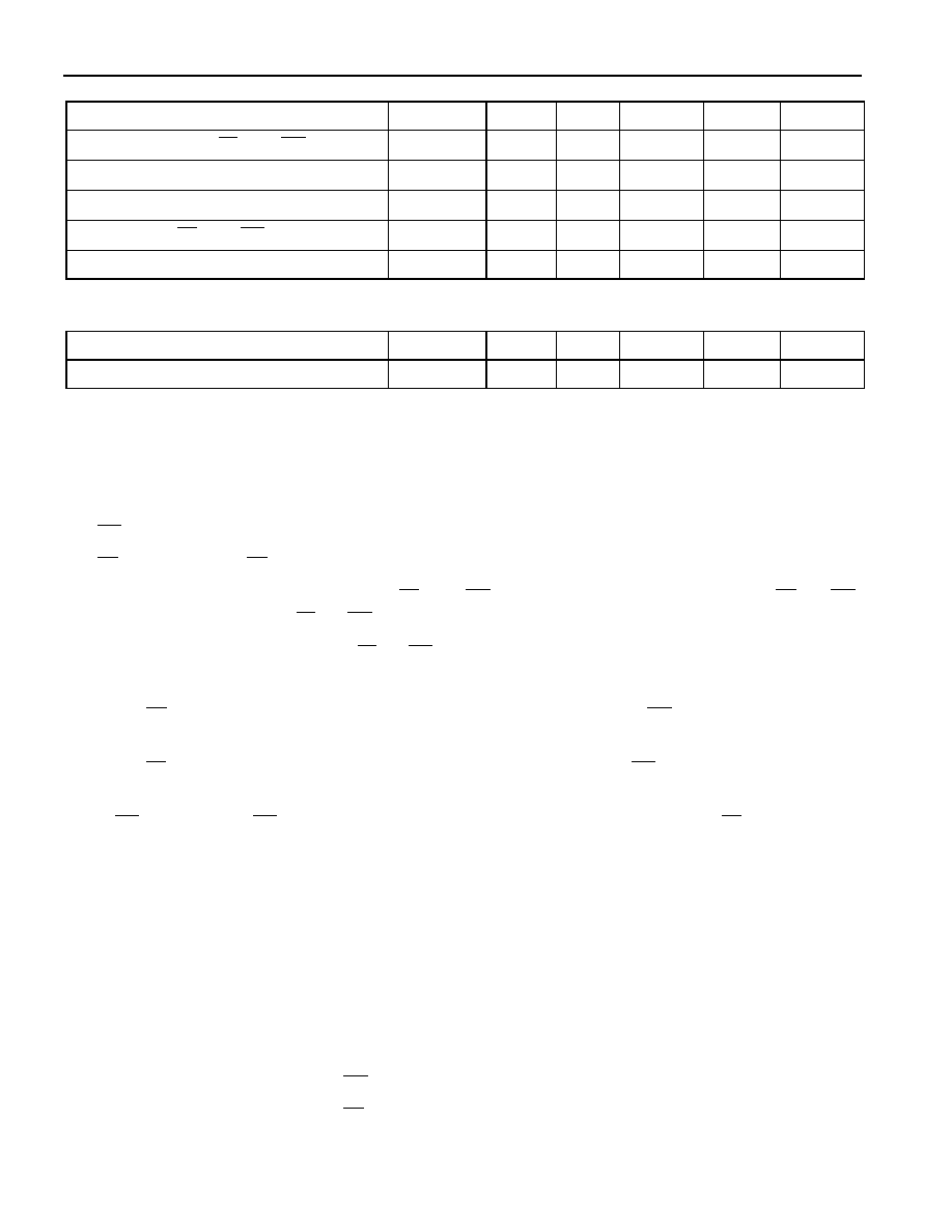
POWER-DOWN/POWER-UP TIMING
(tA: See Note 10)
PARAMETER
SYMBOL
MIN
TYP
MAX
UNITS NOTES
VCC Fail Detect to CE and WE Inactive
tPD
1.5
ms
11
VCC slew from VTP to 0V
tF
150
ms
VCC slew from 0V to VTP
tR
150
ms
VCC Valid to CE and WE Inactive
tPU
2
ms
VCC Valid to End of Write Protection
tREC
125
ms
(tA=25
°C)
PARAMETER
SYMBOL
MIN
TYP
MAX
UNITS NOTES
Expected Data Retention Time
tDR
10
years
9
WARNING:
Under no circumstance are negative undershoots, of any amplitude, allowed when device is in battery
backup mode.
NOTES:
1. WE is high for a Read Cycle.
2. OE = VIH or VIL. If OE = VIH during write cycle, the output buffers remain in a high impedance state.
3. tWP is specified as the logical AND of CE and WE . tWP is measured from the latter of CE or WE
going low to the earlier of CE or WE going high.
4. tDS is measured from the earlier of CE or WE going high.
5. These parameters are sampled with a 5 pF load and are not 100% tested.
6. If the CE low transition occurs simultaneously with or latter than the WE low transition in Write
Cycle 1, the output buffers remain in a high-impedance state during this period.
7. If the CE high transition occurs prior to or simultaneously with the WE high transition, the output
buffers remain in high-impedance state during this period.
8. If WE is low or the WE low transition occurs prior to or simultaneously with the CE low transition,
the output buffers remain in a high-impedance state during this period.
9. Each DS1249 has a built-in switch that disconnects the lithium source until the user first applies VCC.
The expected tDR is defined as accumulative time in the absence of VCC starting from the time power
is first applied by the user. This parameter is assured by component selection, process control, and
design. It is not measured directly during production testing.
10. All AC and DC electrical characteristics are valid over the full operating temperature range. For
commercial products, this range is 0
°C to 70°C. For industrial products (IND), this range is -40°C to
+85
°C.
11. In a power-down condition the voltage on any pin may not exceed the voltage on VCC.
12. tWR1 and tDH1 are measured from WE going high.
13. tWR2 and tDH2 are measured from CE going high.
14. DS1249 modules are recognized by Underwriters Laboratory (U.L.
) under file E99151.
相关PDF资料 |
PDF描述 |
|---|---|
| DS1249Y-100 | 256K X 8 NON-VOLATILE SRAM MODULE, 100 ns, DMA32 |
| DS1250W | 512K X 8 NON-VOLATILE SRAM MODULE, 150 ns, DMA32 |
| DS1250Y | 512K X 8 NON-VOLATILE SRAM MODULE, 70 ns, DMA32 |
| DS1250AB | 512K X 8 NON-VOLATILE SRAM MODULE, 70 ns, DMA32 |
| DS1258AB-70 | 128K X 16 NON-VOLATILE SRAM MODULE, 70 ns, DMA40 |
相关代理商/技术参数 |
参数描述 |
|---|---|
| DS1249Y-70# | 功能描述:NVRAM 2048K NV SRAM RoHS:否 制造商:Maxim Integrated 数据总线宽度:8 bit 存储容量:1024 Kbit 组织:128 K x 8 接口类型:Parallel 访问时间:70 ns 电源电压-最大:5.5 V 电源电压-最小:4.5 V 工作电流:85 mA 最大工作温度:+ 70 C 最小工作温度:0 C 封装 / 箱体:EDIP 封装:Tube |
| DS1249Y-70IND | 功能描述:NVRAM 2048K NV SRAM RoHS:否 制造商:Maxim Integrated 数据总线宽度:8 bit 存储容量:1024 Kbit 组织:128 K x 8 接口类型:Parallel 访问时间:70 ns 电源电压-最大:5.5 V 电源电压-最小:4.5 V 工作电流:85 mA 最大工作温度:+ 70 C 最小工作温度:0 C 封装 / 箱体:EDIP 封装:Tube |
| DS1249Y-70-IND | 制造商:未知厂家 制造商全称:未知厂家 功能描述:NVRAM (Battery Based) |
| DS1249Y-70IND# | 功能描述:NVRAM 2048K NV SRAM RoHS:否 制造商:Maxim Integrated 数据总线宽度:8 bit 存储容量:1024 Kbit 组织:128 K x 8 接口类型:Parallel 访问时间:70 ns 电源电压-最大:5.5 V 电源电压-最小:4.5 V 工作电流:85 mA 最大工作温度:+ 70 C 最小工作温度:0 C 封装 / 箱体:EDIP 封装:Tube |
| DS1249Y-85 | 功能描述:NVRAM 2048K NV SRAM RoHS:否 制造商:Maxim Integrated 数据总线宽度:8 bit 存储容量:1024 Kbit 组织:128 K x 8 接口类型:Parallel 访问时间:70 ns 电源电压-最大:5.5 V 电源电压-最小:4.5 V 工作电流:85 mA 最大工作温度:+ 70 C 最小工作温度:0 C 封装 / 箱体:EDIP 封装:Tube |
发布紧急采购,3分钟左右您将得到回复。