- 您现在的位置:买卖IC网 > PDF目录9370 > DS1340U-3+T&R (Maxim Integrated Products)IC RTC I2C W/CHARGER 3V 8-USOP PDF资料下载
参数资料
| 型号: | DS1340U-3+T&R |
| 厂商: | Maxim Integrated Products |
| 文件页数: | 16/16页 |
| 文件大小: | 0K |
| 描述: | IC RTC I2C W/CHARGER 3V 8-USOP |
| 产品培训模块: | Lead (SnPb) Finish for COTS Obsolescence Mitigation Program |
| 标准包装: | 3,000 |
| 类型: | 时钟/日历 |
| 特点: | 闰年,方波输出,涓流充电器 |
| 时间格式: | HH:MM:SS(24 小时) |
| 数据格式: | YY-MM-DD-dd |
| 接口: | I²C,2 线串口 |
| 电源电压: | 2.7 V ~ 5.5 V |
| 电压 - 电源,电池: | 1.3 V ~ 3.7 V |
| 工作温度: | -40°C ~ 85°C |
| 安装类型: | 表面贴装 |
| 封装/外壳: | 8-TSSOP,8-MSOP(0.118",3.00mm 宽) |
| 供应商设备封装: | 8-uMAX |
| 包装: | 带卷 (TR) |
register increments at midnight. Values that correspond
to the day of week are user-defined but must be
sequential (i.e., if 1 equals Sunday, then 2 equals
Monday, and so on). Illogical time and date entries
result in undefined operation. Bit 7 of register 0 is the
enable oscillator (EOSC) bit. When this bit is set to 1,
the oscillator is disabled. When cleared to 0, the oscil-
lator is enabled. The initial power-up value of EOSC is
0. The clock can be halted whenever the timekeeping
functions are not required, minimizing VBAT current
(IBACKUPDR) when VCC is not applied.
Location 02h is the century/hours register. Bit 7 and bit
6 of the century/hours register are the century-enable
bit (CEB) and the century bit (CB). Setting CEB to logic
1 causes the CB bit to toggle, either from a logic 0 to a
logic 1, or from a logic 1 to a logic 0, when the years
register rolls over from 99 to 00. If CEB is set to logic 0,
CB does not toggle.
When reading or writing the time and date registers,
secondary (user) buffers are used to prevent errors
when the internal registers update. When reading the
time and date registers, the user buffers are synchro-
nized to the internal registers on any START or STOP
and when the register pointer rolls over to zero. The
time information is read from these secondary registers
while the clock continues to run. This eliminates the
need to reread the registers in case the internal regis-
ters update during a read.
The divider chain is reset whenever the seconds regis-
ter is written. Write transfers occur on the acknowledge
from the DS1340. Once the divider chain is reset, to
avoid rollover issues, the remaining time and date reg-
isters must be written within one second.
On a power-on reset (POR), the time and date are set
to 00:00:00 01/01/00 (hh:mm:ss DD/MM/YY) and the
day register is set to 01.
Special-Purpose Registers
The DS1340 has three additional registers (control,
trickle charger, and flag) that control the RTC, trickle
charger, and oscillator flag output.
Control Register (07h)
Bit 7: Output Control (OUT). This bit controls the out-
put level of the FT/OUT pin when the FT bit is set to 0. If
FT = 0, the logic level on the FT/OUT pin is 1 if OUT = 1
and 0 if OUT = 0. The initial power-up OUT value is 1.
Bit 6: Frequency Test (FT). When this bit is 1, the
FT/OUT pin toggles at a 512Hz rate. When FT is written
to 0, the OUT bit controls the state of the FT/OUT pin.
The initial power-up value of FT is 0.
Bit 5: Calibration Sign Bit (S). A logic 1 in this bit indi-
cates positive calibration for the RTC. A 0 indicates
negative calibration for the clock. See the
Clock
Calibration section for a detailed description of the bit
operation. The initial power-up value of S is 0.
Bits 4 to 0: Calibration Bits (CAL4 to CAL0). These
bits can be set to any value between 0 and 31 in binary
form. See the
Clock Calibration section for a detailed
description of the bit operation. The initial power-up
value of CAL0–CAL4 is 0.
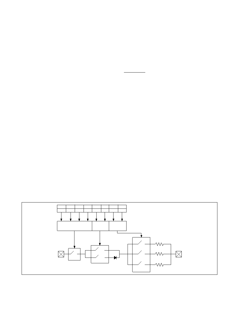
Trickle-Charger Register (08h)
The simplified schematic in Figure 6 shows the basic
components of the trickle charger. The trickle-charge
select (TCS) bits (bits 4–7) control the selection of the
trickle charger. To prevent accidental enabling, only a
I2C RTC with Trickle Charger
Maxim Integrated
9
DS1340
BIT 7
TCS3
1 OF 16 SELECT
NOTE: ONLY 1010b
ENABLES CHARGER
1 OF 2
SELECT
VCC
VBACKUP
R1
250
Ω
TCS0-3 = TRICKLE-CHARGER SELECT
DS0-1 = DIODE SELECT
TOUT0-1 = RESISTOR SELECT
R2
2k
Ω
R3
4k
Ω
1 OF 3
SELECT
BIT 6
TCS2
BIT 5
TCS1
BIT 4
TCS0
BIT 3
DS1
BIT 2
DS0
BIT 1
ROUT1
BIT 0
ROUT0
Figure 6. Trickle Charger Functional Diagram
相关PDF资料 |
PDF描述 |
|---|---|
| DS1338Z-18+T&R | IC RTC 56BYTE NV RAM 1.8V 8-SOIC |
| GTC06CF-20-22P | CONN PLUG 6POS STRAIGHT W/PINS |
| DS1340Z-33+T&R | IC RTC I2C W/CHARGER 3.3V 8-SOIC |
| DS1340Z-3+T&R | IC RTC I2C W/CHARGER 3V 8-SOIC |
| VI-J6J-MZ | CONVERTER MOD DC/DC 36V 25W |
相关代理商/技术参数 |
参数描述 |
|---|---|
| DS1340Z-18 | 功能描述:实时时钟 I2C RTC w/Trickle Charger RoHS:否 制造商:Microchip Technology 功能:Clock, Calendar. Alarm RTC 总线接口:I2C 日期格式:DW:DM:M:Y 时间格式:HH:MM:SS RTC 存储容量:64 B 电源电压-最大:5.5 V 电源电压-最小:1.8 V 最大工作温度:+ 85 C 最小工作温度: 安装风格:Through Hole 封装 / 箱体:PDIP-8 封装:Tube |
| DS1340Z-18+ | 功能描述:实时时钟 I2C RTC w/Trickle Charger RoHS:否 制造商:Microchip Technology 功能:Clock, Calendar. Alarm RTC 总线接口:I2C 日期格式:DW:DM:M:Y 时间格式:HH:MM:SS RTC 存储容量:64 B 电源电压-最大:5.5 V 电源电压-最小:1.8 V 最大工作温度:+ 85 C 最小工作温度: 安装风格:Through Hole 封装 / 箱体:PDIP-8 封装:Tube |
| DS1340Z-3 | 功能描述:实时时钟 I2C RTC w/Trickle Charger RoHS:否 制造商:Microchip Technology 功能:Clock, Calendar. Alarm RTC 总线接口:I2C 日期格式:DW:DM:M:Y 时间格式:HH:MM:SS RTC 存储容量:64 B 电源电压-最大:5.5 V 电源电压-最小:1.8 V 最大工作温度:+ 85 C 最小工作温度: 安装风格:Through Hole 封装 / 箱体:PDIP-8 封装:Tube |
| DS1340Z-3/T&R | 制造商:Maxim Integrated Products 功能描述:REAL TIME CLOCK SERL 8SOIC - Tape and Reel |
| DS1340Z-3+ | 功能描述:实时时钟 I2C RTC w/Trickle Charger RoHS:否 制造商:Microchip Technology 功能:Clock, Calendar. Alarm RTC 总线接口:I2C 日期格式:DW:DM:M:Y 时间格式:HH:MM:SS RTC 存储容量:64 B 电源电压-最大:5.5 V 电源电压-最小:1.8 V 最大工作温度:+ 85 C 最小工作温度: 安装风格:Through Hole 封装 / 箱体:PDIP-8 封装:Tube |
发布紧急采购,3分钟左右您将得到回复。