- 您现在的位置:买卖IC网 > PDF目录295503 > DS17285S-3+T&R (MAXIM INTEGRATED PRODUCTS INC) 3V/5V Real-Time Clock PDF资料下载
参数资料
| 型号: | DS17285S-3+T&R |
| 厂商: | MAXIM INTEGRATED PRODUCTS INC |
| 元件分类: | XO, clock |
| 英文描述: | 3V/5V Real-Time Clock |
| 中文描述: | 1 TIMER(S), REAL TIME CLOCK, PDSO24 |
| 封装: | SO-24 |
| 文件页数: | 14/38页 |
| 文件大小: | 411K |
| 代理商: | DS17285S-3+T&R |
第1页第2页第3页第4页第5页第6页第7页第8页第9页第10页第11页第12页第13页当前第14页第15页第16页第17页第18页第19页第20页第21页第22页第23页第24页第25页第26页第27页第28页第29页第30页第31页第32页第33页第34页第35页第36页第37页第38页
DS17285/DS17287
21 of 38
EXTENDED CONTROL REGISTERS
Two extended control registers are provided to supply controls and status information for the extended
features offered by the DS17285/DS17287. These are designated as extended control registers 4A and 4B
and are located in register bank 1, locations 04AH and 04BH, respectively. The functions of the bits
within these registers are described as follows.
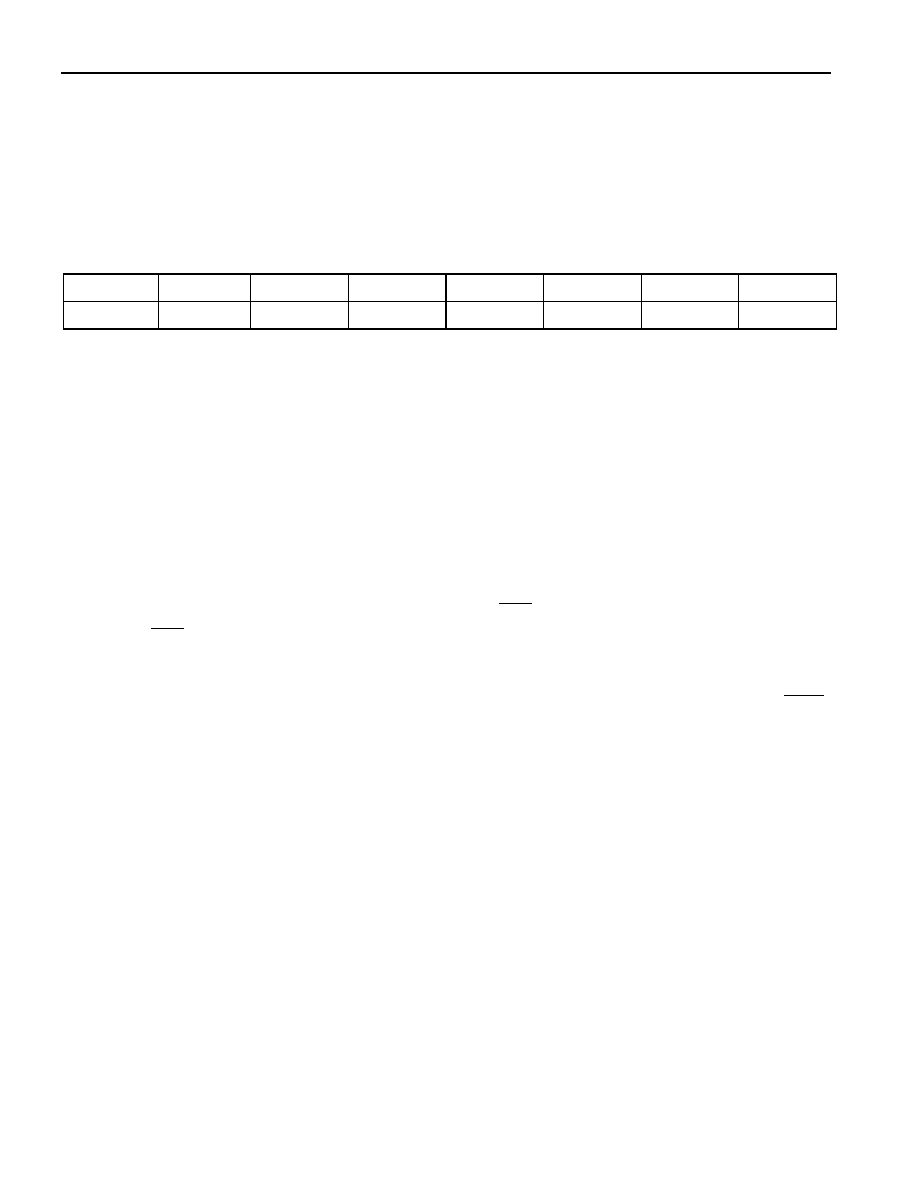
EXTENDED CONTROL REGISTER 4A
MSB
LSB
BIT 7
BIT 6
BIT 5
BIT 4
BIT 3
BIT 2
BIT 1
BIT 0
VRT2
INCR
BME
*
PAB
RF
WF
KF
VRT2 – Valid RAM and Time 2. This status bit gives the condition of the auxiliary batter. It is set to a
logic 1 condition when the external lithium battery is connected to the VBAUX. If this bit is read as a logivc
0, the external battery should be replaced.
INCR – Increment in Progress Status. This bit is set to a 1 when an increment to the time/date registers
is in progress and the alarm checks are being made. INCR is set to a 1 at 122s before the update cycle
starts and is cleared to 0 at the end of each update cycle.
BME – Burst Mode Enable. The burst mode enable bit allows the extended user RAM address registers
to automatically increment for consecutive reads and writes. When BME is set to a logic 1, the automatic
incrementing is enabled and when BME is set to a logic 0, the automatic incrementing is disabled.
PAB – Power-Active Bar-Control. When this bit is 0, the PWR pin is in the active low state. When this
bit is 1, the PWR pin is in the high-impedance state. This bit can be written to a logic 1 or 0 by the user. If
either WF and WIE = 1 or KF and KSE = 1, the PAB bit is cleared to 0.
RF – Ram Clear Flag. This bit is set to a logic 1 when a high-to-low transition occurs on the RCLR
input if RCE = 1. The RF bit is cleared by writing it to a logic 0. This bit can also be written to a logic 1
to force an interrupt condition.
WF – Wake-Up Alarm Flag. This bit is set to 1 when a wake-up alarm condition occurs or when the
user writes it to a 1. WF is cleared by writing it to a 0.
KF – Kickstart Flag. This bit is set to a 1 when a kickstart condition occurs or when the user writes it to
a 1. This bit is cleared by writing it to a logic 0.
*Reserved bits. These bits are reserved for future use by Dallas Semiconductor. They can be read and
written, but have no affect on operation.
相关PDF资料 |
PDF描述 |
|---|---|
| DS17285S-5+T&R | 3V/5V Real-Time Clock |
| DS1743P-85IND+ | Y2K-Compliant, Nonvolatile Timekeeping RAMs |
| DS1743P-C01+ | Y2K-Compliant, Nonvolatile Timekeeping RAMs |
| DS1744-70+ | Y2K-Compliant, Nonvolatile Timekeeping RAMs |
| DS1744-70IND+ | Y2K-Compliant, Nonvolatile Timekeeping RAMs |
相关代理商/技术参数 |
参数描述 |
|---|---|
| DS17285S-5 | 制造商:Rochester Electronics LLC 功能描述: 制造商:Maxim Integrated Products 功能描述: |
| DS17285S-5/T&R | 制造商:Maxim Integrated Products 功能描述:IC RTC 5V 2K NV RAM 24-SOIC |
| DS17285S-5/T&R | 功能描述:实时时钟 RoHS:否 制造商:Microchip Technology 功能:Clock, Calendar. Alarm RTC 总线接口:I2C 日期格式:DW:DM:M:Y 时间格式:HH:MM:SS RTC 存储容量:64 B 电源电压-最大:5.5 V 电源电压-最小:1.8 V 最大工作温度:+ 85 C 最小工作温度: 安装风格:Through Hole 封装 / 箱体:PDIP-8 封装:Tube |
| DS17285S-5+ | 功能描述:实时时钟 3V/5V RTC K Multiplexed Kick-S RoHS:否 制造商:Microchip Technology 功能:Clock, Calendar. Alarm RTC 总线接口:I2C 日期格式:DW:DM:M:Y 时间格式:HH:MM:SS RTC 存储容量:64 B 电源电压-最大:5.5 V 电源电压-最小:1.8 V 最大工作温度:+ 85 C 最小工作温度: 安装风格:Through Hole 封装 / 箱体:PDIP-8 封装:Tube |
| DS17285S-5+T&R | 制造商:Maxim Integrated Products 功能描述:REAL TIME CLOCK MULTIPLEXED 2KBYTE 24SOIC - Tape and Reel 制造商:Maxim Integrated Products 功能描述:Maxim Integrated DS17285S-5+T&R Real Time Clocks (RTC) 制造商:Maxim Integrated Products 功能描述:IC RTC 5V 2K NV RAM 24-SOIC |
发布紧急采购,3分钟左右您将得到回复。