- 您现在的位置:买卖IC网 > PDF目录1994 > DS17285S-3NT (Maxim Integrated Products)IC RTC 3V 2K NV RAM 24-SOIC PDF资料下载
参数资料
| 型号: | DS17285S-3NT |
| 厂商: | Maxim Integrated Products |
| 文件页数: | 4/31页 |
| 文件大小: | 0K |
| 描述: | IC RTC 3V 2K NV RAM 24-SOIC |
| 标准包装: | 1,000 |
| 类型: | 时钟/日历 |
| 特点: | 警报器,夏令时,闰年,NVSRAM,方波输出 |
| 存储容量: | 2KB |
| 时间格式: | HH:MM:SS(12/24 小时) |
| 数据格式: | YY-MM-DD-dd |
| 接口: | 并联 |
| 电源电压: | 2.7 V ~ 3.7 V |
| 电压 - 电源,电池: | 2.5 V ~ 3.7 V |
| 工作温度: | -40°C ~ 85°C |
| 安装类型: | 表面贴装 |
| 封装/外壳: | 24-SOIC(0.295",7.50mm 宽) |
| 供应商设备封装: | 24-SOIC W |
| 包装: | 带卷 (TR) |
第1页第2页第3页当前第4页第5页第6页第7页第8页第9页第10页第11页第12页第13页第14页第15页第16页第17页第18页第19页第20页第21页第22页第23页第24页第25页第26页第27页第28页第29页第30页第31页
DS17285/DS17287/DS17485/DS17487/DS17885/DS17887
Power-Down/Power-Up
Considerations
The RTC function continues to operate, and all the
RAM, time, calendar, and alarm memory locations
remain nonvolatile regardless of the level of the VCC
input. VBAT or VBAUX must remain within the minimum
and maximum limits when VCC is not applied. When
VCC falls below VPF, the device inhibits all access,
putting the part into a low-power mode. When VCC is
applied and exceeds VPF (power-fail trip point), the
device becomes accessible after tREC, if the oscillator
is running and the oscillator countdown chain is not in
reset (Register A). This time period allows the system to
stabilize after power is applied. If the oscillator is not
enabled, the oscillator enable bit is enabled on power-
up, and the device becomes immediately accessible.
Power Control
The power control function is provided by a precise,
temperature-compensated voltage reference and a
comparator circuit that monitors the VCC level. The
device is fully accessible and data can be written and
read when VCC is greater than VPF. However, when
VCC falls below VPF, the device inhibits read and write
access. If VPF is less than VBAT, the device power is
switched from VCC to the higher of VBAT or VBAUX
when VCC drops below VPF. If VPF is greater than the
higher of VBAT or VBAUX, the device power is switched
from VCC to the higher of VBAT or VBAUX when VCC
drops below the higher backup source. The registers
are maintained from the VBAT or VBAUX source until
VCC is returned to nominal levels. After VCC returns
above VPF, read and write access is allowed after tREC.
Time, Calendar, and Alarm
Locations
The time and calendar information is obtained by read-
ing the appropriate register bytes. The time, calendar,
and alarm are set or initialized by writing the appropri-
ate register bytes. The contents of the 12 time, calen-
dar, and alarm bytes can be either binary or
binary-coded decimal (BCD) format. Tables 3A and 3B
show the BCD and binary formats of the 12 time, date,
and alarm registers, control registers A to D, plus the
two extended registers that reside in bank 1 only (bank
0 and bank 1 switching is explained later in this text).
The day-of-week register increments at midnight, incre-
menting from 1 through 7. The day-of-week register is
used by the daylight saving function, and so the value
1 is defined as Sunday. The date at the end of the
month is automatically adjusted for months with fewer
than 31 days, including correction for leap years.
Before writing the internal time, calendar, and alarm
registers, the SET bit in Register B should be written to
logic 1 to prevent updates from occurring while access
is being attempted. In addition to writing the 12 time,
calendar, and alarm registers in a selected format
(binary or BCD), the data mode bit (DM) of Register B
must be set to the appropriate logic level. All 12 time,
calendar, and alarm bytes must use the same data
mode. The set bit in Register B should be cleared after
the data mode bit has been written to allow the real
time clock to update the time and calendar bytes. Once
initialized, the real time clock makes all updates in the
selected mode. The data mode cannot be changed
without reinitializing the 12 data bytes. Tables 3A and
3B show the BCD and binary formats of the 12 time,
calendar, and alarm locations.
The 24-12 bit cannot be changed without reinitializing
the hour locations. When the 12-hour format is selected,
the high order bit of the hours byte represents PM when
it is logic 1. The time, calendar, and alarm bytes are
always accessible because they are double-buffered.
Once per second, the eight bytes are advanced by one
second and checked for an alarm condition.
If a read of the time and calendar data occurs during
an update, a problem exists where seconds, minutes,
hours, etc., may not correlate. The probability of read-
ing incorrect time and calendar data is low. Several
methods of avoiding any possible incorrect time and
calendar reads are covered later in this text.
Real-Time Clocks
12
____________________________________________________________________
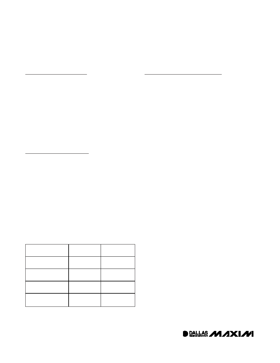
Table 2. Power Control
SUPPLY CONDITION
READ/WRITE
ACCESS
POWERED BY
VCC < VPF, VCC <
(VBAT | VBAUX)
No
VBAT or VBAUX
VCC < VPF, VCC >
(VBAT | VBAUX)
No
VCC
VCC > VPF, VCC <
(VBAT | VBAUX)
Yes
VCC
VCC > VPF, VCC >
(VBAT | VBAUX)
Yes
VCC
相关PDF资料 |
PDF描述 |
|---|---|
| DS1742-100IND | IC RTC RAM Y2K 5V 100NS 24-EDIP |
| DS1743P-70+ | IC RTC RAM Y2K 5V 70NS 34-PCM |
| DS1744-70IND | IC RTC RAM Y2K 5V 70NS 28-EDIP |
| DS1746-70IND | IC RTC RAM Y2K 5V 70NS 32-EDIP |
| DS1747W-120IND | IC RTC RAM Y2K 3.3V 120NS 32EDIP |
相关代理商/技术参数 |
参数描述 |
|---|---|
| DS17285S-5 | 制造商:Rochester Electronics LLC 功能描述: 制造商:Maxim Integrated Products 功能描述: |
| DS17285S-5/T&R | 制造商:Maxim Integrated Products 功能描述:IC RTC 5V 2K NV RAM 24-SOIC |
| DS17285S-5/T&R | 功能描述:实时时钟 RoHS:否 制造商:Microchip Technology 功能:Clock, Calendar. Alarm RTC 总线接口:I2C 日期格式:DW:DM:M:Y 时间格式:HH:MM:SS RTC 存储容量:64 B 电源电压-最大:5.5 V 电源电压-最小:1.8 V 最大工作温度:+ 85 C 最小工作温度: 安装风格:Through Hole 封装 / 箱体:PDIP-8 封装:Tube |
| DS17285S-5+ | 功能描述:实时时钟 3V/5V RTC K Multiplexed Kick-S RoHS:否 制造商:Microchip Technology 功能:Clock, Calendar. Alarm RTC 总线接口:I2C 日期格式:DW:DM:M:Y 时间格式:HH:MM:SS RTC 存储容量:64 B 电源电压-最大:5.5 V 电源电压-最小:1.8 V 最大工作温度:+ 85 C 最小工作温度: 安装风格:Through Hole 封装 / 箱体:PDIP-8 封装:Tube |
| DS17285S-5+T&R | 制造商:Maxim Integrated Products 功能描述:REAL TIME CLOCK MULTIPLEXED 2KBYTE 24SOIC - Tape and Reel 制造商:Maxim Integrated Products 功能描述:Maxim Integrated DS17285S-5+T&R Real Time Clocks (RTC) 制造商:Maxim Integrated Products 功能描述:IC RTC 5V 2K NV RAM 24-SOIC |
发布紧急采购,3分钟左右您将得到回复。