- 您现在的位置:买卖IC网 > PDF目录20033 > DS1863E+T&R (Maxim Integrated)IC LASR CTRLR 1CHAN 5.5V 16TSSOP PDF资料下载
参数资料
| 型号: | DS1863E+T&R |
| 厂商: | Maxim Integrated |
| 文件页数: | 13/62页 |
| 文件大小: | 0K |
| 描述: | IC LASR CTRLR 1CHAN 5.5V 16TSSOP |
| 产品培训模块: | Lead (SnPb) Finish for COTS Obsolescence Mitigation Program |
| 标准包装: | 1,000 |
| 类型: | 激光二极管控制器 |
| 通道数: | 1 |
| 电源电压: | 2.85 V ~ 5.5 V |
| 电流 - 电源: | 5mA |
| 电流 - 偏置: | 1.2mA |
| 工作温度: | -40°C ~ 95°C |
| 封装/外壳: | 16-TSSOP(0.173",4.40mm 宽) |
| 供应商设备封装: | 16-TSSOP |
| 包装: | 带卷 (TR) |
| 安装类型: | 表面贴装 |
第1页第2页第3页第4页第5页第6页第7页第8页第9页第10页第11页第12页当前第13页第14页第15页第16页第17页第18页第19页第20页第21页第22页第23页第24页第25页第26页第27页第28页第29页第30页第31页第32页第33页第34页第35页第36页第37页第38页第39页第40页第41页第42页第43页第44页第45页第46页第47页第48页第49页第50页第51页第52页第53页第54页第55页第56页第57页第58页第59页第60页第61页第62页
�� �
�
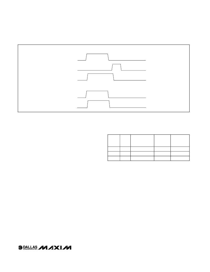
�Burst-Mode� PON� Controller�
�With� Integrated� Monitoring�
�TX-F� LATCHED� OPERATION�
�DETECTION� OF�
�TX-F� FAULT�
�TX-D� OR�
�TX-F� RESET�
�TX-F�
�TX-F� NON-LATCHED� OPERATION�
�DETECTION� OF�
�TX-F� FAULT�
�TX-F�
�Figure� 5.� DS1863� TX-F� Timing.�
�FETG� output� is� always� latched� in� case� it� is� triggered� by�
�an� unmasked� alarm� condition.� Its� output� polarity� is� pro-�
�grammable� to� allow� an� external� N� or� P� MOSFET� to� open�
�FETG� and� MOD� and� BIAS� Outputs� as� a�
�Function� of� TX-D� and� Alarm� Sources�
�during� alarms� to� shut� off� the� laser� diode� current.� If� the�
�FETG� output� triggers� indicating� the� DS1863� is� in� shut-�
�down,� then� it� requires� TX-D,� soft� TX-D,� or� cycling� power�
�to� be� reset.� Under� all� conditions� when� the� analog� outputs�
�are� re-initialized� after� being� disabled,� all� the� alarms� with�
�the� exception� of� the� V� CC� low� ADC� alarm� will� be� cleared.�
�The� V� CC� low� alarm� must� remain� active� to� prevent� the� out-�
�V� CC� >�
�V� POA�
�Yes�
�Yes�
�Yes�
�TX-D�
�0�
�0�
�1�
�NON-MASKED�
�FETG� ALARM�
�0�
�1�
�X�
�FETG�
�FETG� DIR�
�FETG� DIR�
�FETG� DIR�
�MOD� AND�
�BIAS�
�OUTPUTS�
�Enabled�
�Disabled�
�Disabled�
�put� from� attempting� to� operate� when� inadequate� V� CC�
�exists� to� operate� the� laser� driver.� Once� adequate� V� CC� is�
�present� to� clear� the� V� CC� low� alarm,� the� outputs� will� be�
�enabled� following� the� same� sequence� as� power� up.�
�As� mentioned� before� the� FETG� is� an� output� used� to� dis-�
�able� the� laser� current� via� a� series� N� or� P� MOSFET.� This�
�requires� that� the� FETG� output� is� capable� of� sinking� or�
�sourcing� current.� Because� the� DS1863� will� not� know� if� it�
�should� sink� or� source� current� before� V� CC� exceeds�
�V� POA� ,� which� triggers� the� EE� recall,� this� output� will� be�
�high� impedance� when� V� CC� is� below� V� POA� .� (see� “� Low�
�Voltage� Operation� ”� section� for� details� and� diagram).�
�The� application� circuit� must� use� a� pull-up� or� pull-down�
�resistor� on� this� pin� that� pulls� FETG� to� the� alarm/shut-�
�down� state� (high� for� a� PMOS,� low� for� a� NMOS).� Once�
�V� CC� is� above� V� POA� ,� the� DS1863� will� pull� the� FETG� out-�
�put� to� the� state� determined� by� the� FETG� DIR� bit� (Table�
�02h,� Register� 89h).� FETG� DIR� will� be� 0� if� an� NMOS� is�
�used� and� 1� if� a� PMOS� is� used.�
�Determining� Alarm� Causes�
�Using� The� I� 2� C� Interface�
�To� determine� the� cause� of� the� TX-F� or� FETG� alarm,� the�
�system� processor� can� read� the� DS1863� ’� s� Alarm� Trap�
�Bytes� (ATB)� through� the� I� 2� C� interface� (in� Table� 01h).� The�
�ATB� have� a� bit� for� each� alarm.� Any� time� an� alarm� occurs,�
�regardless� of� the� mask� bit� ’� s� state,� the� DS1863� sets� the�
�corresponding� bit� in� the� ATB.� Active� ATB� bits� will� remain�
�set� until� written� to� zeros� via� the� I� 2� C� interface.� On� power�
�up� the� ATB� will� be� zeros� until� alarms� dictate� otherwise.�
�Die� Identification�
�DS1863� will� have� an� ID� hard� coded� to� its� die.� Two� reg-�
�isters� (Table� 02h� bytes� 86h� –� 87h)� are� assigned� for� this�
�feature.� Byte� 86h� will� read� 63h� to� identify� the� part� as� the�
�DS1863,� byte� 87h� will� read� to� A1h� (for� A1� die� revision).�
�Low-Voltage� Operation�
�The� DS1863� contains� two� Power-On� Reset� (POR)� lev-�
�els.� The� lower� level� is� a� Digital� POR� (V� POD� )� and� the�
�____________________________________________________________________�
�13�
�相关PDF资料 |
PDF描述 |
|---|---|
| QPI-10LZ-01 | IC HOT SWAP EMI FILTER 10LGA |
| GMM44DRES | CONN EDGECARD 88POS .156 EYELET |
| VE-J0W-CY-B1 | CONVERTER MOD DC/DC 5.5V 50W |
| T86C225K025EBSS | CAP TANT 2.2UF 25V 10% 2312 |
| ABC31DRXH-S734 | CONN EDGECARD 62POS DIP .100 SLD |
相关代理商/技术参数 |
参数描述 |
|---|---|
| DS1863K | 功能描述:电源管理IC开发工具 RoHS:否 制造商:Maxim Integrated 产品:Evaluation Kits 类型:Battery Management 工具用于评估:MAX17710GB 输入电压: 输出电压:1.8 V |
| DS1863T+ | 制造商:Maxim Integrated Products 功能描述:- Rail/Tube |
| DS1864 | 制造商:DALLAS 制造商全称:Dallas Semiconductor 功能描述:SFP Laser Controller and Diagnostic IC |
| DS1864K | 功能描述:电源管理IC开发工具 RoHS:否 制造商:Maxim Integrated 产品:Evaluation Kits 类型:Battery Management 工具用于评估:MAX17710GB 输入电压: 输出电压:1.8 V |
| DS1864T | 制造商:Maxim Integrated Products 功能描述:DUAL TMP CTRL DAC+MONITORS,QFN - Rail/Tube |
发布紧急采购,3分钟左右您将得到回复。