- 您现在的位置:买卖IC网 > PDF目录18728 > DS1870E-010+ (Maxim Integrated)IC CNTRLR RF POWER AMP 16TSSOP PDF资料下载
参数资料
| 型号: | DS1870E-010+ |
| 厂商: | Maxim Integrated |
| 文件页数: | 24/28页 |
| 文件大小: | 0K |
| 描述: | IC CNTRLR RF POWER AMP 16TSSOP |
| 产品培训模块: | Lead (SnPb) Finish for COTS Obsolescence Mitigation Program |
| 标准包装: | 96 |
| RF 型: | 手机 |
| 封装/外壳: | 16-TSSOP(0.173",4.40mm 宽) |
| 供应商设备封装: | 16-TSSOP |
| 包装: | 管件 |
| 产品目录页面: | 1431 (CN2011-ZH PDF) |
第1页第2页第3页第4页第5页第6页第7页第8页第9页第10页第11页第12页第13页第14页第15页第16页第17页第18页第19页第20页第21页第22页第23页当前第24页第25页第26页第27页第28页
�� �
�
�LDMOS� RF� Power-Amplifier� Bias�
�Controller�
�TABLE� 2� (TEMP� LUT� FOR� POT� 1)�
�Bytes� 80h–C7h�
�POT1�
�<R/W><NV><00h>The� unsigned� base� value� for� POT1.�
�TABLE� 3� (TEMP� LUT� FOR� POT� 2)�
�Bytes� 80h–C7h�
�POT2�
�<R/W><NV><00h>The� unsigned� base� value� for� POT2.�
�TABLE� 4� (DRAIN� LUT� FOR� POT� 1)�
�Bytes� 80h–B8h�
�POT1� Off�
�<R/W><NV><00h>The� signed� 2’s� complement� offset� value� for� POT1.�
�TABLE� 5� (DRAIN� LUT� FOR� POT� 2)�
�Bytes� 80h–B8h�
�POT2� Off�
�<R/W><NV><00h>The� signed� 2’s� complement� offset� value� for� POT2.�
�I� 2� C� Definitions�
�The� following� terminology� is� commonly� used� to�
�describe� I� 2� C� data� transfers.�
�Master� device:� The� master� device� controls� the� slave�
�devices� on� the� bus.� The� master� device� generates� SCL�
�clock� pulses,� and� start� and� stop� conditions.�
�Slave� devices:� Slave� devices� send� and� receive� data� at�
�the� master’s� request.�
�Bus� idle� or� not� busy:� Time� between� stop� and� start�
�conditions� when� both� SDA� and� SCL� are� inactive� and� in�
�their� logic� high� states.� When� the� bus� is� idle,� it� often� initi-�
�ates� a� low-power� mode� for� slave� devices.�
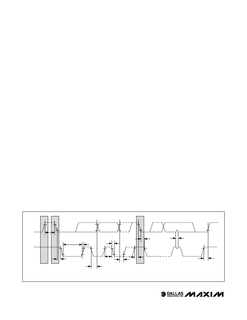
�Start� condition:� A� start� condition� is� generated� by� the�
�master� to� initiate� a� new� data� transfer� with� a� slave.�
�Transitioning� SDA� from� high� to� low� while� SCL� remains�
�high� generates� a� start� condition.� See� the� timing� dia-�
�gram� for� applicable� timing.�
�SDA�
�Stop� condition:� A� stop� condition� is� generated� by� the�
�master� to� end� a� data� transfer� with� a� slave.� Transitioning�
�SDA� from� low� to� high� while� SCL� remains� high� gener-�
�ates� a� stop� condition.� See� the� timing� diagram� for�
�applicable� timing.�
�Repeated� start� condition:� The� master� can� use� a�
�repeated� start� condition� at� the� end� of� one� data� transfer�
�to� indicate� that� it� will� immediately� initiate� a� new� data�
�transfer� following� the� current� one.� Repeated� starts� are�
�commonly� used� during� read� operations� to� identify� a�
�specific� memory� address� to� begin� a� data� transfer.� A�
�repeated� start� condition� is� issued� identically� to� a� nor-�
�mal� start� condition.� See� the� timing� diagram� for� applica-�
�ble� timing.�
�Bit� write:� Transitions� of� SDA� must� occur� during� the� low�
�state� of� SCL.� The� data� on� SDA� must� remain� valid� and�
�unchanged� during� the� entire� high� pulse� of� SCL� plus� the�
�t� BUF�
�t� HD:STA�
�t� SP�
�SCL�
�t� LOW�
�t� R�
�t� F�
�t� HD:STA�
�t� HIGH�
�t� SU:STA�
�STOP�
�START�
�t� SU:DAT�
�REPEATED�
�START�
�t� SU:STO�
�t� HD:DAT�
�NOTE:� TIMING� IS� REFERENCED� TO� V� IL(MAX)� AND� V� IH(MIN)� .�
�Figure� 3.� I� 2� C� Timing� Diagram�
�24�
�____________________________________________________________________�
�相关PDF资料 |
PDF描述 |
|---|---|
| GLEB01A2B | SWITCH SIDE-ROTRY ROLL SNAP SPDT |
| GLEB01A5B | SWITCH SIDE-ROTRY ROLL SNAP SPDT |
| F5KA833M0D4MG-Z | FILTER SAW 833MHZ CDMA2000 |
| MAX2530ETI+ | IC LNA/MIXER CELL/PCS/GPS 28TQFN |
| UPC2746TB-E3-A | MMIC AMP 1.5GHZ SOT-363 |
相关代理商/技术参数 |
参数描述 |
|---|---|
| DS1870E-010+ | 功能描述:特殊用途放大器 LDMOS RF Power-Amp Bias Controller RoHS:否 制造商:Texas Instruments 通道数量:Single 共模抑制比(最小值): 输入补偿电压: 工作电源电压:3 V to 5.5 V 电源电流:5 mA 最大功率耗散: 最大工作温度:+ 70 C 最小工作温度:- 40 C 安装风格:SMD/SMT 封装 / 箱体:QFN-20 封装:Reel |
| DS1870E-010+T&R | 制造商:Maxim Integrated Products 功能描述:LDMOS RF PWR-AMP BIAS CNTRLR 16TSSOP - Tape and Reel 制造商:Maxim Integrated Products 功能描述:IC RF PWR CNTRL PA 16TSSOP |
| DS1870E-010+T&R | 功能描述:特殊用途放大器 LDMOS RF Power-Amp Bias Controller RoHS:否 制造商:Texas Instruments 通道数量:Single 共模抑制比(最小值): 输入补偿电压: 工作电源电压:3 V to 5.5 V 电源电流:5 mA 最大功率耗散: 最大工作温度:+ 70 C 最小工作温度:- 40 C 安装风格:SMD/SMT 封装 / 箱体:QFN-20 封装:Reel |
| DS1870K | 制造商:Maxim Integrated Products 功能描述:DS1870 EVALUATION KIT - Bulk |
| DS1873 | 制造商:MAXIM 制造商全称:Maxim Integrated Products 功能描述:SFP+ Controller with Analog LDD Interface |
发布紧急采购,3分钟左右您将得到回复。