- 您现在的位置:买卖IC网 > PDF目录11671 > DS1876T+ (Maxim Integrated Products)IC CTRLR SFP DUAL LDD 28TQFN PDF资料下载
参数资料
| 型号: | DS1876T+ |
| 厂商: | Maxim Integrated Products |
| 文件页数: | 14/69页 |
| 文件大小: | 0K |
| 描述: | IC CTRLR SFP DUAL LDD 28TQFN |
| 产品培训模块: | Lead (SnPb) Finish for COTS Obsolescence Mitigation Program |
| 标准包装: | 60 |
| 类型: | SFP 激光控制器 |
| 输入类型: | 逻辑 |
| 输出类型: | 逻辑 |
| 接口: | I²C |
| 电流 - 电源: | 10mA |
| 安装类型: | 表面贴装 |
| 封装/外壳: | 28-WFQFN 裸露焊盘 |
| 供应商设备封装: | 28-TQFN-EP(5x5) |
| 包装: | 管件 |
第1页第2页第3页第4页第5页第6页第7页第8页第9页第10页第11页第12页第13页当前第14页第15页第16页第17页第18页第19页第20页第21页第22页第23页第24页第25页第26页第27页第28页第29页第30页第31页第32页第33页第34页第35页第36页第37页第38页第39页第40页第41页第42页第43页第44页第45页第46页第47页第48页第49页第50页第51页第52页第53页第54页第55页第56页第57页第58页第59页第60页第61页第62页第63页第64页第65页第66页第67页第68页第69页
21
Maxim Integrated
SFP Controller with Dual LDD Interface
DS1876
always the second byte transmitted during a write
operation following the slave address byte.
I2C Protocol
See Figure 13 for an example of I2C timing.
Writing a Single Byte to a Slave: The master must
generate a START condition, write the slave address
byte (R/W = 0), write the memory address, write
the byte of data, and generate a STOP condition.
Remember that the master must read the slave’s
acknowledgement during all byte write operations.
Writing Multiple Bytes to a Slave: To write multiple
bytes to a slave, the master generates a START condi-
tion, writes the slave address byte (R/W = 0), writes
the memory address, writes up to 8 data bytes, and
generates a STOP condition. The DS1876 writes 1 to
8 bytes (one page or row) with a single write trans-
action. This is internally controlled by an address
counter that allows data to be written to consecutive
addresses without transmitting a memory address
before each data byte is sent. The address counter
limits the write to one 8-byte page (one row of the
memory map). Attempts to write to additional pages
of memory without sending a STOP condition between
pages result in the address counter wrapping around
to the beginning of the present row.
For example: A 3-byte write starts at address 06h and
writes three data bytes (11h, 22h, and 33h) to three
“consecutive” addresses. The result is that addresses
06h and 07h would contain 11h and 22h, respec-
tively, and the third data byte, 33h, would be written
to address 00h.
To prevent address wrapping from occurring, the
master must send a STOP condition at the end of
the page, then wait for the bus-free or EEPROM write
time to elapse. Then the master can generate a new
START condition and write the slave address byte
(R/W = 0) and the first memory address of the next
memory row before continuing to write data.
Acknowledge Polling: Any time a EEPROM page is
written, the DS1876 requires the EEPROM write time
(tWR) after the STOP condition to write the contents of
the page to EEPROM. During the EEPROM write time,
the DS1876 does not acknowledge its slave address
because it is busy. It is possible to take advantage
of that phenomenon by repeatedly addressing the
DS1876, which allows the next page to be written
as soon as the DS1876 is ready to receive the data.
The alternative to acknowledge polling is to wait for
maximum period of tWR to elapse before attempting
to write again to the DS1876.
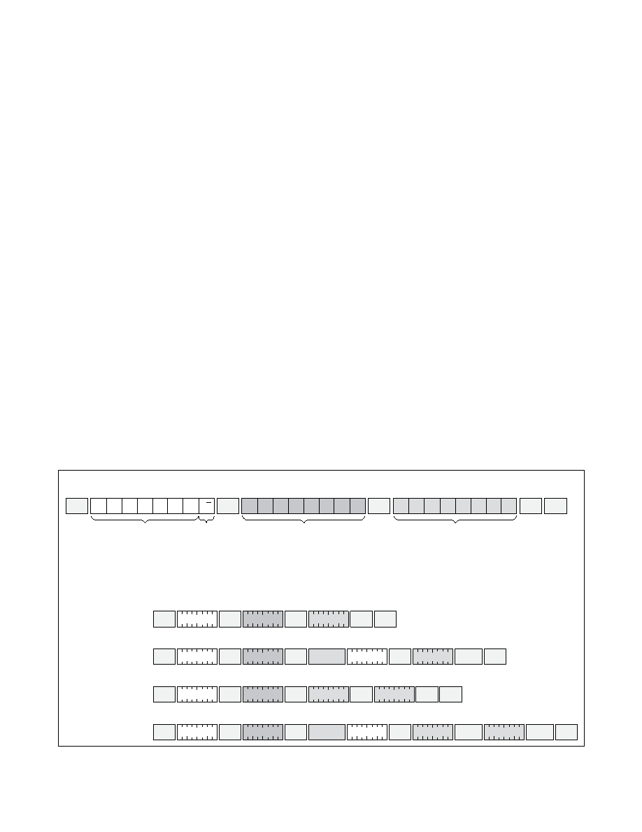
Figure 13. Example I2C Timing
START
STOP
SLAVE
ACK
SLAVE
ACK
STOP
SINGLE-BYTE WRITE
-WRITE 00h TO REGISTER BAh
TWO-BYTE WRITE
-WRITE 01h AND 75h TO
REGISTERS C8h AND C9h
SINGLE-BYTE READ
-READ REGISTER BAh
TWO-BYTE READ
-READ C8h AND C9h
REPEATED
START
MASTER
NACK
1 0 1 0 0 0 1 0
A2h
1 0 1 1 1 0 1 0
BAh
SLAVE
ACK
START
SLAVE
ACK
1 0 1 0 0 0 1 0
A2h
1 0 1 0 0 0 1 1
A3h
1 0 1 1 1 0 1 0
BAh
SLAVE
ACK
SLAVE
ACK
STOP
0 0 0 0 0 0 0 0
00h
STOP
SLAVE
ACK
STOP
0 1 1 1 0 1 0 1
75h
START
SLAVE
ACK
1 0 1 0 0 0 1 0
A2h
1 1 0 0 1 0 0 0
C8h
SLAVE
ACK
SLAVE
ACK
0 0 0 0 0 0 0 1
01h
SLAVE
ACK
DATA IN BAh
DATA
REPEATED
START
MASTER
ACK
START
SLAVE
ACK
1 0 1 0 0 0 1 0
A2h
1 0 1 0 0 0 1 1
A3h
1 1 0 0 1 0 0 0
C8h
SLAVE
ACK
SLAVE
ACK
DATA IN C8h
DATA
MASTER
NACK
DATA IN C9h
DATA
EXAMPLE I2C TRANSACTIONS WITH A2h AS THE SLAVE ADDRESS
*IF ASEL IS 0, THE SLAVE ADDRESS IS A0h FOR THE AUXILIARY MEMORY AND A2h/B2h FOR THE MAIN MEMORY.
IF ASEL = 1, THE SLAVE ADDRESS IS DETERMINED BY TABLE 02h, REGISTER 8Bh FOR THE MAIN MEMORY. THE AUXILIARY MEMORY CONTINUES TO BE ADDRESSED AT A0h, EXCEPT WHEN THE PROGRAMMED
ADDRESS FOR THE MAIN MEMORY IS A0h.
TYPICAL I2C WRITE TRANSACTION
A)
C)
B)
D)
MSB
LSB
b7
b6
b5
b4
b3
b2
b1
b0
REGISTER ADDRESS
MSB
LSB
b7
b6
b5
b4
b3
b2
b1
b0
DATA
SLAVE
ACK
SLAVE
ACK
SLAVE
ADDRESS*
X
0
1
R/W
MSB
LSB
READ/
WRITE
相关PDF资料 |
PDF描述 |
|---|---|
| VI-BVJ-IX-F4 | CONVERTER MOD DC/DC 36V 75W |
| 221128-1 | PLUG,COMMERCIAL BNC |
| VI-BV3-IX-F1 | CONVERTER MOD DC/DC 24V 75W |
| VI-BV2-IX-F3 | CONVERTER MOD DC/DC 15V 75W |
| 227161-3 | CONN JACK BNC R/A 50OHM PCB AU |
相关代理商/技术参数 |
参数描述 |
|---|---|
| DS1876T+ | 功能描述:ADC / DAC多通道 SFP+ Controller w/ Dual LDD Interface RoHS:否 制造商:Texas Instruments 转换速率: 分辨率:8 bit 接口类型:SPI 电压参考: 电源电压-最大:3.6 V 电源电压-最小:2 V 最大工作温度:+ 85 C 安装风格:SMD/SMT 封装 / 箱体:VQFN-40 |
| DS1876T+T&R | 制造商:Maxim Integrated Products 功能描述:SFP CTRLR W/DUAL LDD INTERFACE TQFN - Tape and Reel 制造商:Maxim Integrated Products 功能描述:IC CTRLR SFP DUAL LDD 28TQFN |
| DS1876T+T&R | 功能描述:ADC / DAC多通道 SFP+ Controller w/ Dual LDD Interface RoHS:否 制造商:Texas Instruments 转换速率: 分辨率:8 bit 接口类型:SPI 电压参考: 电源电压-最大:3.6 V 电源电压-最小:2 V 最大工作温度:+ 85 C 安装风格:SMD/SMT 封装 / 箱体:VQFN-40 |
| DS1876T+TR | 制造商:MAXIM 制造商全称:Maxim Integrated Products 功能描述:SFP Controller with Dual LDD Interface |
| DS1877 | 制造商:MAXIM 制造商全称:Maxim Integrated Products 功能描述:SFP Controller for Dual Rx Interface |
发布紧急采购,3分钟左右您将得到回复。