- 您现在的位置:买卖IC网 > PDF目录11671 > DS1876T+ (Maxim Integrated Products)IC CTRLR SFP DUAL LDD 28TQFN PDF资料下载
参数资料
| 型号: | DS1876T+ |
| 厂商: | Maxim Integrated Products |
| 文件页数: | 7/69页 |
| 文件大小: | 0K |
| 描述: | IC CTRLR SFP DUAL LDD 28TQFN |
| 产品培训模块: | Lead (SnPb) Finish for COTS Obsolescence Mitigation Program |
| 标准包装: | 60 |
| 类型: | SFP 激光控制器 |
| 输入类型: | 逻辑 |
| 输出类型: | 逻辑 |
| 接口: | I²C |
| 电流 - 电源: | 10mA |
| 安装类型: | 表面贴装 |
| 封装/外壳: | 28-WFQFN 裸露焊盘 |
| 供应商设备封装: | 28-TQFN-EP(5x5) |
| 包装: | 管件 |
第1页第2页第3页第4页第5页第6页当前第7页第8页第9页第10页第11页第12页第13页第14页第15页第16页第17页第18页第19页第20页第21页第22页第23页第24页第25页第26页第27页第28页第29页第30页第31页第32页第33页第34页第35页第36页第37页第38页第39页第40页第41页第42页第43页第44页第45页第46页第47页第48页第49页第50页第51页第52页第53页第54页第55页第56页第57页第58页第59页第60页第61页第62页第63页第64页第65页第66页第67页第68页第69页
15
Maxim Integrated
SFP Controller with Dual LDD Interface
DS1876
The ADC results (after right-shifting, if used) are com-
pared to the alarm and warning thresholds after each
conversion, and the corresponding alarms are set that
can be used to trigger the TXFOUT output. These ADC
thresholds are user programmable, as are the masking
registers that can be used to prevent the alarms from trig-
gering the TXFOUT output.
ADC Timing
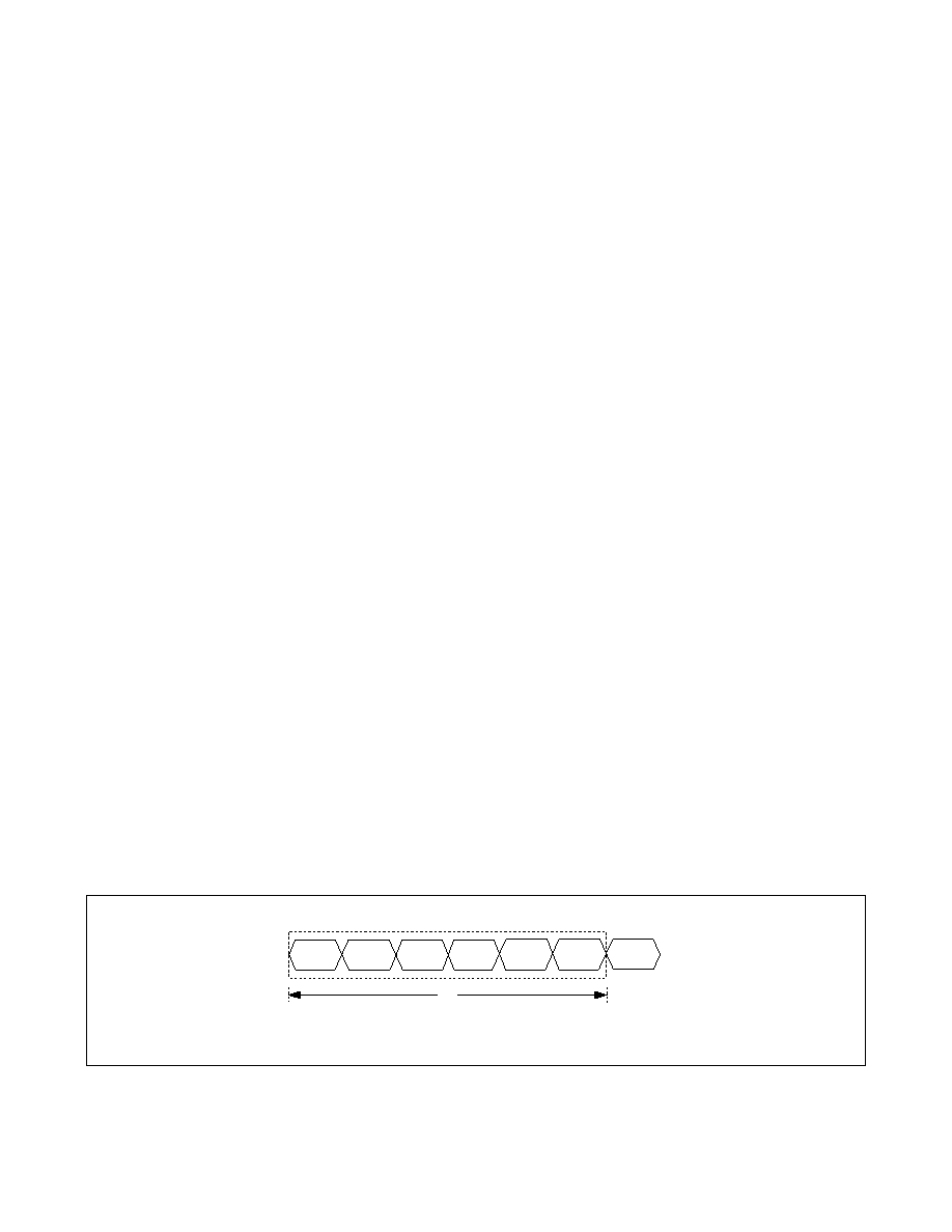
There are six analog channels that are digitized in a
round-robin fashion in the order as shown in Figure 4.
The total time required to convert all six channels is tRR
(see the Analog Voltage Monitoring Characteristics table
for details).
Right-Shifting ADC Result
If the weighting of the ADC digital reading must conform
to a predetermined full-scale (PFS) value defined by
a standard’s specification (e.g., SFF-8472), then right-
shifting can be used to adjust the PFS analog measure-
ment range while maintaining the weighting of the ADC
results. The DS1876’s range is wide enough to cover all
requirements; when the maximum input value is P 1/2
the FS value, right-shifting can be used to obtain greater
accuracy. For instance, the maximum voltage might be
1/8 the specified PFS value, so only 1/8 of the converter’s
range is effective over this range. An alternative is to cali-
brate the ADC’s full-scale range to 1/8 the readable PFS
value and use a right-shift value of 3. With this implemen-
tation, the resolution of the measurement is increased by
a factor of 8, and because the result is digitally divided
by 8 by right-shifting, the bit weight of the measurement
still meets the standard’s specification (i.e., SFF-8472).
The right-shift operation on the ADC result is carried
out based on the contents of right-shift control registers
(Table 02h, Registers 8Eh
-8Fh) in EEPROM. Four analog
channels—PMON1, PMON2, BMON1, and BMON2—
each have 3 bits allocated to set the number of right-
shifts. Up to seven right-shift operations are allowed and
are executed as a part of every conversion before the
results are compared to the high and low alarm levels, or
loaded into their corresponding measurement registers
(Lower Memory, Registers 64h–6Bh). This is true during
the setup of internal calibration as well as during subse-
quent data conversions.
Low-Voltage Operation
The DS1876 contains two power-on reset (POR) levels.
The lower level is a digital POR (POD) and the higher
level is an analog POR (POA). At startup, before the sup-
ply voltage rises above POA, the outputs are disabled,
all SRAM locations are set to their defaults, shadowed
EEPROM (SEE) locations are zero, and all analog cir-
cuitry is disabled. When VCC reaches POA, the SEE is
recalled, and the analog circuitry is enabled. While VCC
remains above POA, the device is in its normal operating
state, and it responds based on its nonvolatile configu-
ration. If during operation VCC falls below POA, but is
still above POD, the SRAM retains the SEE settings from
the first SEE recall, but the device analog is shut down
and the outputs disabled. If the supply voltage recovers
back above POA, the device immediately resumes nor-
mal operation. If the supply voltage falls below POD, the
device SRAM is placed in its default state and another
SEE recall is required to reload the nonvolatile settings.
The EEPROM recall occurs the next time VCC next
exceeds POA. Figure 5 shows the sequence of events
as the voltage varies.
Any time VCC is above POD, the I2C interface can be
used to determine if VCC is below the POA level. This
is accomplished by checking the RDYB bit in the status
byte (Lower Memory, Register 6Eh). RDYB is set when
VCC is below POA; when VCC rises above POA, RDYB
is timed (within 500Fs) to go to 0, at which point the part
is fully functional.
Figure 4. ADC Round-Robin Timing
TEMP
VCC
BMON1
BMON2
PMON1
PMON2
TEMP
ONE ROUND-ROBIN ADC CYCLE
tRR
NOTE: IF THE VCC LO ALARM IS ENABLED AT POWER-UP, THE ADC ROUND-ROBIN TIMING CYCLES BETWEEN TEMPERATURE AND VCC ONLY UNTIL VCC IS ABOVE THE VCC LO
ALARM THRESHOLD. THIS ALSO OCCURS IF THERE ARE BOTH A TXD1 EVENT AND A TXD2 EVENT UNDER THE SAME CONDITIONS AS PREVIOUSLY MENTIONED.
相关PDF资料 |
PDF描述 |
|---|---|
| VI-BVJ-IX-F4 | CONVERTER MOD DC/DC 36V 75W |
| 221128-1 | PLUG,COMMERCIAL BNC |
| VI-BV3-IX-F1 | CONVERTER MOD DC/DC 24V 75W |
| VI-BV2-IX-F3 | CONVERTER MOD DC/DC 15V 75W |
| 227161-3 | CONN JACK BNC R/A 50OHM PCB AU |
相关代理商/技术参数 |
参数描述 |
|---|---|
| DS1876T+ | 功能描述:ADC / DAC多通道 SFP+ Controller w/ Dual LDD Interface RoHS:否 制造商:Texas Instruments 转换速率: 分辨率:8 bit 接口类型:SPI 电压参考: 电源电压-最大:3.6 V 电源电压-最小:2 V 最大工作温度:+ 85 C 安装风格:SMD/SMT 封装 / 箱体:VQFN-40 |
| DS1876T+T&R | 制造商:Maxim Integrated Products 功能描述:SFP CTRLR W/DUAL LDD INTERFACE TQFN - Tape and Reel 制造商:Maxim Integrated Products 功能描述:IC CTRLR SFP DUAL LDD 28TQFN |
| DS1876T+T&R | 功能描述:ADC / DAC多通道 SFP+ Controller w/ Dual LDD Interface RoHS:否 制造商:Texas Instruments 转换速率: 分辨率:8 bit 接口类型:SPI 电压参考: 电源电压-最大:3.6 V 电源电压-最小:2 V 最大工作温度:+ 85 C 安装风格:SMD/SMT 封装 / 箱体:VQFN-40 |
| DS1876T+TR | 制造商:MAXIM 制造商全称:Maxim Integrated Products 功能描述:SFP Controller with Dual LDD Interface |
| DS1877 | 制造商:MAXIM 制造商全称:Maxim Integrated Products 功能描述:SFP Controller for Dual Rx Interface |
发布紧急采购,3分钟左右您将得到回复。