- 您现在的位置:买卖IC网 > PDF目录11706 > DS1884T+ (Maxim Integrated Products)IC SFP PON ONU CTRLR 24TQFN PDF资料下载
参数资料
| 型号: | DS1884T+ |
| 厂商: | Maxim Integrated Products |
| 文件页数: | 13/92页 |
| 文件大小: | 0K |
| 描述: | IC SFP PON ONU CTRLR 24TQFN |
| 产品培训模块: | Lead (SnPb) Finish for COTS Obsolescence Mitigation Program |
| 产品变化通告: | DS1884 Series Discontinuation 03/Aug/2012 |
| 标准包装: | 28 |
| 系列: | * |
第1页第2页第3页第4页第5页第6页第7页第8页第9页第10页第11页第12页当前第13页第14页第15页第16页第17页第18页第19页第20页第21页第22页第23页第24页第25页第26页第27页第28页第29页第30页第31页第32页第33页第34页第35页第36页第37页第38页第39页第40页第41页第42页第43页第44页第45页第46页第47页第48页第49页第50页第51页第52页第53页第54页第55页第56页第57页第58页第59页第60页第61页第62页第63页第64页第65页第66页第67页第68页第69页第70页第71页第72页第73页第74页第75页第76页第77页第78页第79页第80页第81页第82页第83页第84页第85页第86页第87页第88页第89页第90页第91页第92页
DS1884
SFP and PON ONU Controller
with Digital LDD Interface
20
Maxim Integrated
Additionally, TXB, TXP, RSSIC, and RSSIF can right-shift
results as described in the Right-Shifting ADC Result sec-
tion. This allows customers with specified ADC ranges to
calibrate the ADC input gain by a factor of 2n to measure
small signals (thereby reducing the full scale by a factor
of 2n). The DS1884 can then right-shift the results by n
bits (effectively multiplying by a factor of 1/2n) to maintain
the bit weight of their specification. See the Right-Shifting
Functionality) sections for more information.
Alarms and Warnings
The ADC results (after right-shifting, if used) are com-
pared to the alarm and warning thresholds after each
conversion, and the corresponding alarms and/or warn-
ings are set, which can be programmed to create the
internal signal TXFINT. The status of TXFINT can be read
in A2h Lower Memory, Register 71h. TXFINT is one of
the signals used to trigger TXFOUT. TXFOUT can be
programmed to cause TXDOUT outputs. These ADC
thresholds are user-programmable, as are the masking
registers that can be used to prevent the alarms from
triggering the TXFOUT and TXDOUT outputs.
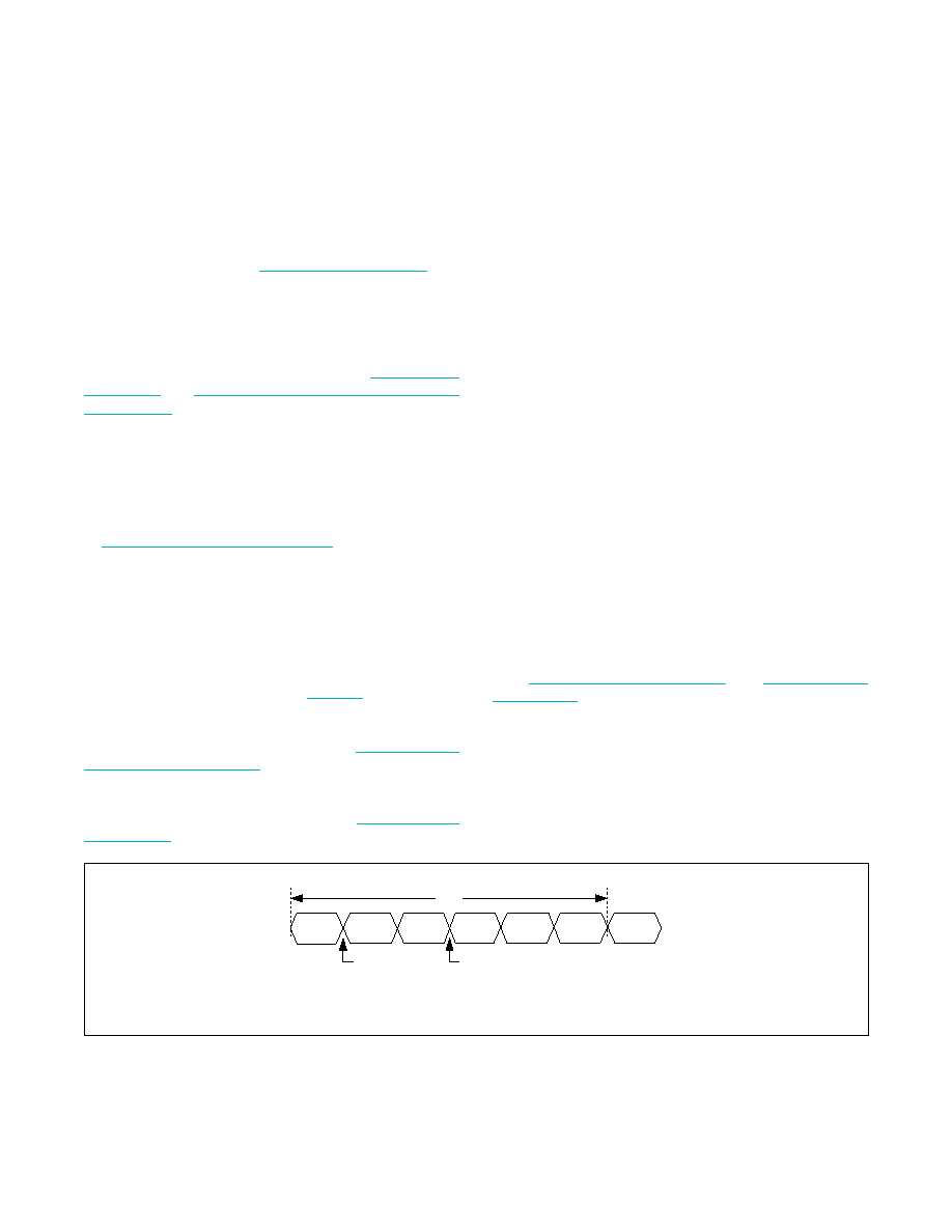
ADC Timing
Five analog channels are digitized in a round-robin
fashion in the order as shown in Figure 2. RSSI is mea-
sured twice to obtain coarse and fine measurements
(RSSIC and RSSIF, respectively). The total time required
Monitoring Characteristics table for details). After each
TXMON conversion, a 3-wire communication is initi-
ated to toggle the MON_SEL bit (bit 6 in the MAX3710’s
TXCTRL2 register, programmed through A2h Table 02h,
Register E5h, bit 6). This causes the laser driver to
alternate sending laser bias (TXB) and laser power
(TXP) signals to the DS1884’s TXMON input.
Right-Shifting ADC Result
If the weighting of the ADC digital reading must conform to
a predetermined full-scale (PFS) value defined by a stan-
dard’s specification (e.g., SFF-8472), then right-shifting can
be used to adjust the PFS analog measurement range while
maintaining the weighting of the ADC results. The DS1884’s
range is wide enough to cover all requirements; when the
maximum input value is ≤ 1/2 of the full-scale value, right-
shifting can be used to obtain greater accuracy.
For instance, the maximum voltage might be 1/8 the
specified PFS value, so only 1/8 the converter’s range is
effective over this range. An alternative is to calibrate the
ADC’s full-scale range to 1/8 the readable PFS value (by
calibrating an input gain of about 8 using the scale regis-
ters) and use a right-shift value of 3. With this implemen-
tation, the resolution of the measurement is increased by
a factor of 8, and because the result is digitally divided
by 8 by right-shifting, the bit weight of the measurement
still meets the standard’s specification (i.e., SFF-8472).
The right-shift operation on the ADC result is carried
out based on the contents of right-shift control regis-
ters (A2h Table 02h, Register 8Eh and A2h Table 02h,
Register 8Fh) in EEPROM. TXB, TXP, RSSIC, and RSSIF
have 3 bits allocated to set the number of right-shifts.
Up to seven right-shift operations are allowed and are
executed as a part of every conversion before the results
are compared to the high and low alarm levels, or loaded
into their corresponding measurement registers (Lower
Memory, Registers 64h–69h). This is true during the
setup of internal calibration as well as during subsequent
data conversions.
Figure 2. ADC Round-Robin Timing
TEMP
VCC
TXB
RSSIC
TOGGLE MON_SEL
RSSIF
TXP
TEMP
tRR
NOTE: IF VCC LO ALARM OR WARNING IS ENABLED AT POWER-UP, THE ADC ROUND-ROBIN TIMING CYCLES BETWEEN TEMPERATURE AND VCC ONLY UNTIL VCC IS ABOVE
THE VCC LO ALARM THRESHOLD.
TOGGLE MON_SEL
相关PDF资料 |
PDF描述 |
|---|---|
| MS27467E25A35SA | CONN PLUG 128POS STRAIGHT W/SCKT |
| GRM216R71H223KA01J | CAP CER 0.022UF 50V 10% X7R 0805 |
| VE-BVM-IX-F3 | CONVERTER MOD DC/DC 10V 75W |
| VE-BVM-IX-F2 | CONVERTER MOD DC/DC 10V 75W |
| GRM216F51H223ZA01D | CAP CER 0.022UF 50V Y5V 0805 |
相关代理商/技术参数 |
参数描述 |
|---|---|
| DS1884T+ | 功能描述:ADC / DAC多通道 SFP+ Controller w/ Digi LDD Interface RoHS:否 制造商:Texas Instruments 转换速率: 分辨率:8 bit 接口类型:SPI 电压参考: 电源电压-最大:3.6 V 电源电压-最小:2 V 最大工作温度:+ 85 C 安装风格:SMD/SMT 封装 / 箱体:VQFN-40 |
| DS1884T+T | 功能描述:ADC / DAC多通道 SFP+ Controller w/ Digi LDD Interface RoHS:否 制造商:Texas Instruments 转换速率: 分辨率:8 bit 接口类型:SPI 电压参考: 电源电压-最大:3.6 V 电源电压-最小:2 V 最大工作温度:+ 85 C 安装风格:SMD/SMT 封装 / 箱体:VQFN-40 |
| DS1886 | 制造商:未知厂家 制造商全称:未知厂家 功能描述:带有数字LDD接口的SFP和PON ONU控制器 |
| DS1886_V1 | 制造商:MAXIM 制造商全称:Maxim Integrated Products 功能描述:SFP and PON ONU Controller with Digital LDD Interface |
| DS1886T+ | 功能描述:接口 - 专用 PON ONU/SFP CTRLR W/DIG LDD INT RoHS:否 制造商:Texas Instruments 产品类型:1080p60 Image Sensor Receiver 工作电源电压:1.8 V 电源电流:89 mA 最大功率耗散: 最大工作温度:+ 85 C 安装风格:SMD/SMT 封装 / 箱体:BGA-59 |
发布紧急采购,3分钟左右您将得到回复。