- 您现在的位置:买卖IC网 > PDF目录9759 > DS21348GN (Maxim Integrated Products)IC LIU LN T1/E1/J1 3.3V 49-BGA PDF资料下载
参数资料
| 型号: | DS21348GN |
| 厂商: | Maxim Integrated Products |
| 文件页数: | 6/76页 |
| 文件大小: | 0K |
| 描述: | IC LIU LN T1/E1/J1 3.3V 49-BGA |
| 产品培训模块: | Lead (SnPb) Finish for COTS Obsolescence Mitigation Program |
| 标准包装: | 416 |
| 类型: | 线路接口装置(LIU) |
| 驱动器/接收器数: | 1/1 |
| 规程: | T1/E1/J1 |
| 电源电压: | 3.135 V ~ 3.465 V |
| 安装类型: | 表面贴装 |
| 封装/外壳: | 49-LFBGA,CSPBGA |
| 供应商设备封装: | 49-CSBGA(7x7) |
| 包装: | 托盘 |
第1页第2页第3页第4页第5页当前第6页第7页第8页第9页第10页第11页第12页第13页第14页第15页第16页第17页第18页第19页第20页第21页第22页第23页第24页第25页第26页第27页第28页第29页第30页第31页第32页第33页第34页第35页第36页第37页第38页第39页第40页第41页第42页第43页第44页第45页第46页第47页第48页第49页第50页第51页第52页第53页第54页第55页第56页第57页第58页第59页第60页第61页第62页第63页第64页第65页第66页第67页第68页第69页第70页第71页第72页第73页第74页第75页第76页
DS21348/DS21Q348
14 of 76
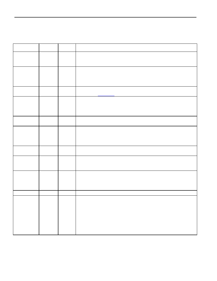
2.1 Pin Descriptions
Table 2-5. Pin Descriptions in Parallel Port Mode (Sorted by Pin Name,
DS21348T Pin Numbering)
NAME
PIN
I/O
FUNCTION
A0 to A4
11 to 7
I
Address Bus. In nonmultiplexed bus operation (BIS1 = 0, BIS0 =
1), serves as the address bus. In multiplexed bus operation (BIS1 =
0, BIS0 = 0), these pins are not used and should be tied low.
ALE (AS)
4
I
Address Latch Enable (Address Strobe). When using the parallel
port (BIS1 = 0) in multiplexed bus mode (BIS0 = 0), serves to
demultiplex the bus on a positive-going edge. In nonmultiplexed bus
mode (BIS0 = 1), should be tied low.
BIS0/BIS1
32/33
I
Bus Interface Select Bits 0 and 1. Used to select bus interface
option. See Table 2-1 for details.
BPCLK
31
O
Backplane Clock. A 16.384MHz, 8.192MHz, 4.096MHz, or
2.048MHz clock output that is referenced to RCLK selectable via
CCR5.7 and CCR5.6. In hardware mode, defaults to 16.384MHz
output.
CS
1
I
Chip Select, Active Low. This active-low signal must be low to
read or write to the device.
D0/AD0 to
D7/AD7
19 to 12
I/O
Data Bus/Address/Data Bus. In nonmultiplexed bus operation
(BIS1 = 0, BIS0 = 1), serves as the data bus. In multiplexed bus
operation (BIS1 = 0, BIS0 = 0), serves as an 8-bit multiplexed
address/data bus.
HRST
29
I
Hardware Reset, Active Low. Bringing
HRST low resets the
DS21348, setting all control bits to their default state of all zeros.
INT
23
O
Interrupt, Active Low. Flags host controller during conditions and
change of conditions defined in the Status Register. Active low,
open drain output.
MCLK
30
I
Master Clock. A 2.048MHz (±50ppm) clock source with TTL
levels is applied at this pin. This clock is used internally for both
clock/data recovery and for jitter attenuation. Use of a T1 1.544MHz
clock source is optional.
N/A
—
I
Not Assigned. Should be tied low.
PBEO
24
O
PRBS Bit Error Output. The receiver will constantly search for a
215-1 or a 220-1 PRBS depending on the ETS bit setting (CCR1.7).
Remains high if out of synchronization with the PRBS pattern. Goes
low when synchronized to the PRBS pattern. Any errors in the
received pattern after synchronization will cause a positive going
pulse (with same period as E1 or T1 clock) synchronous with
RCLK. PRBS bit errors can also be reported to the ECR1 and ECR2
registers by setting CCR6.2 to a logic 1.
相关PDF资料 |
PDF描述 |
|---|---|
| VI-241-MX-F3 | CONVERTER MOD DC/DC 12V 75W |
| MAX214EPI+ | IC TXRX RS-232 PROG 28-DIP |
| MAX214EWI+ | IC TXRX RS-232 PROG 28-SOIC |
| HI5767/2IA | CONV A/D 10BIT 20MSPS 28-SOIC |
| VI-242-MX-F4 | CONVERTER MOD DC/DC 15V 75W |
相关代理商/技术参数 |
参数描述 |
|---|---|
| DS21348GN+ | 功能描述:网络控制器与处理器 IC 3.3V E1/T1/J1 Line Interface RoHS:否 制造商:Micrel 产品:Controller Area Network (CAN) 收发器数量: 数据速率: 电源电流(最大值):595 mA 最大工作温度:+ 85 C 安装风格:SMD/SMT 封装 / 箱体:PBGA-400 封装:Tray |
| DS21348GNB | 功能描述:网络控制器与处理器 IC RoHS:否 制造商:Micrel 产品:Controller Area Network (CAN) 收发器数量: 数据速率: 电源电流(最大值):595 mA 最大工作温度:+ 85 C 安装风格:SMD/SMT 封装 / 箱体:PBGA-400 封装:Tray |
| DS21348GN-C01 | 功能描述:网络控制器与处理器 IC 3.3V E1/T1/J1 Line Interface RoHS:否 制造商:Micrel 产品:Controller Area Network (CAN) 收发器数量: 数据速率: 电源电流(最大值):595 mA 最大工作温度:+ 85 C 安装风格:SMD/SMT 封装 / 箱体:PBGA-400 封装:Tray |
| DS21348T | 功能描述:网络控制器与处理器 IC 3.3V E1/T1/J1 Line Interface RoHS:否 制造商:Micrel 产品:Controller Area Network (CAN) 收发器数量: 数据速率: 电源电流(最大值):595 mA 最大工作温度:+ 85 C 安装风格:SMD/SMT 封装 / 箱体:PBGA-400 封装:Tray |
| DS21348T+ | 功能描述:网络控制器与处理器 IC 3.3V E1/T1/J1 Line Interface RoHS:否 制造商:Micrel 产品:Controller Area Network (CAN) 收发器数量: 数据速率: 电源电流(最大值):595 mA 最大工作温度:+ 85 C 安装风格:SMD/SMT 封装 / 箱体:PBGA-400 封装:Tray |
发布紧急采购,3分钟左右您将得到回复。