- 您现在的位置:买卖IC网 > PDF目录9759 > DS21348GN (Maxim Integrated Products)IC LIU LN T1/E1/J1 3.3V 49-BGA PDF资料下载
参数资料
| 型号: | DS21348GN |
| 厂商: | Maxim Integrated Products |
| 文件页数: | 7/76页 |
| 文件大小: | 0K |
| 描述: | IC LIU LN T1/E1/J1 3.3V 49-BGA |
| 产品培训模块: | Lead (SnPb) Finish for COTS Obsolescence Mitigation Program |
| 标准包装: | 416 |
| 类型: | 线路接口装置(LIU) |
| 驱动器/接收器数: | 1/1 |
| 规程: | T1/E1/J1 |
| 电源电压: | 3.135 V ~ 3.465 V |
| 安装类型: | 表面贴装 |
| 封装/外壳: | 49-LFBGA,CSPBGA |
| 供应商设备封装: | 49-CSBGA(7x7) |
| 包装: | 托盘 |
第1页第2页第3页第4页第5页第6页当前第7页第8页第9页第10页第11页第12页第13页第14页第15页第16页第17页第18页第19页第20页第21页第22页第23页第24页第25页第26页第27页第28页第29页第30页第31页第32页第33页第34页第35页第36页第37页第38页第39页第40页第41页第42页第43页第44页第45页第46页第47页第48页第49页第50页第51页第52页第53页第54页第55页第56页第57页第58页第59页第60页第61页第62页第63页第64页第65页第66页第67页第68页第69页第70页第71页第72页第73页第74页第75页第76页
DS21348/DS21Q348
15 of 76
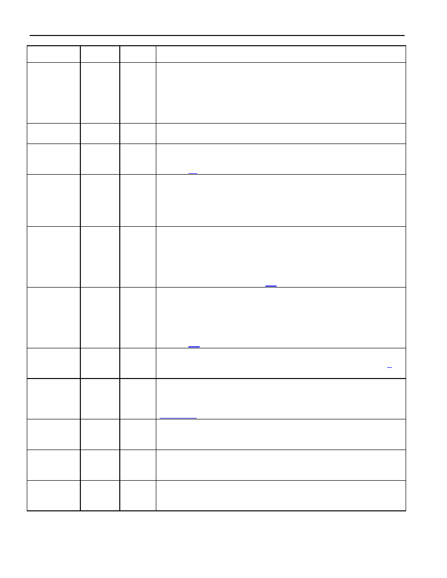
NAME
PIN
I/O
FUNCTION
PBTS
44
I
Parallel Bus Type Select. When using the parallel port (BIS1 = 0),
set high to select Motorola bus timing, set low to select Intel bus
timing. This pin controls the function of the
RD (DS), ALE (AS),
and
WR (R/W) pins. If PBTS = 1 and BIS1 = 0, then these pins
assume the Motorola function listed in parentheses (). In serial port
mode, this pin should be tied low.
RCLK
40
O
Receive Clock. Buffered recovered clock from the line.
Synchronous to MCLK in absence of signal at RTIP and RRING.
RD (DS)
2
I
Read Input (Data Strobe), Active Low. DS is active low when in
nonmultiplexed, Motorola mode. See the bus timing diagrams in
Section 11.
RCL/
LOTC
25
O
Receive Carrier Loss/Loss of Transmit Clock. An output which
will toggle high during a receive carrier loss (CCR2.7 = 0) or will
toggle high if the TCLK pin has not been toggled for 5
sec ± 2
sec (CCR2.7 = 1). CCR2.7 defaults to logic 0 when in hardware
mode.
RNEG
39
O
Receive Negative Data. Updated on the rising edge (CCR2.0 = 0)
or the falling edge (CCR2.0 = 1) of RCLK with the bipolar data out
of the line interface. Set NRZE (CCR1.6) to a one for NRZ
applications. In NRZ mode, data will be output on RPOS while a
received error will cause a positive-going pulse synchronous with
RCLK at RNEG. See Section 6.4 for details.
RPOS
38
O
Receive Positive Data. Updated on the rising edge (CCR2.0 = 0) or
the falling edge (CCR2.0 = 1) of RCLK with bipolar data out of the
line interface. Set NRZE (CCR1.6) to a one for NRZ applications. In
NRZ mode, data will be output on RPOS while a received error will
cause a positive-going pulse synchronous with RCLK at RNEG. See
Section 6.4 for details.
RTIP/
RRING
27/28
I
Receive Tip and Ring. Analog inputs for clock recovery circuitry.
These pins connect via a 1:1 transformer to the line. See Section 5
for details.
TCLK
43
I
Transmit Clock. A 2.048MHz or 1.544MHz primary clock. Used to
clock data through the transmit side formatter. Can be sourced
internally by MCLK or RCLK. See Common Control Register 1 and
TEST
26
I
Tri-State Control. Set high to tri-state all outputs and I/O pins
(including the parallel control port). Set low for normal operation.
Useful in board level testing.
TNEG
42
I
Transmit Negative Data. Sampled on the falling edge (CCR2.1 =
0) or the rising edge (CCR2.1 = 1) of TCLK for data to be
transmitted out onto the line.
TPOS
41
I
Transmit Positive Data. Sampled on the falling edge (CCR2.1 = 0)
or the rising edge (CCR2.1 = 1) of TCLK for data to be transmitted
out onto the line.
相关PDF资料 |
PDF描述 |
|---|---|
| VI-241-MX-F3 | CONVERTER MOD DC/DC 12V 75W |
| MAX214EPI+ | IC TXRX RS-232 PROG 28-DIP |
| MAX214EWI+ | IC TXRX RS-232 PROG 28-SOIC |
| HI5767/2IA | CONV A/D 10BIT 20MSPS 28-SOIC |
| VI-242-MX-F4 | CONVERTER MOD DC/DC 15V 75W |
相关代理商/技术参数 |
参数描述 |
|---|---|
| DS21348GN+ | 功能描述:网络控制器与处理器 IC 3.3V E1/T1/J1 Line Interface RoHS:否 制造商:Micrel 产品:Controller Area Network (CAN) 收发器数量: 数据速率: 电源电流(最大值):595 mA 最大工作温度:+ 85 C 安装风格:SMD/SMT 封装 / 箱体:PBGA-400 封装:Tray |
| DS21348GNB | 功能描述:网络控制器与处理器 IC RoHS:否 制造商:Micrel 产品:Controller Area Network (CAN) 收发器数量: 数据速率: 电源电流(最大值):595 mA 最大工作温度:+ 85 C 安装风格:SMD/SMT 封装 / 箱体:PBGA-400 封装:Tray |
| DS21348GN-C01 | 功能描述:网络控制器与处理器 IC 3.3V E1/T1/J1 Line Interface RoHS:否 制造商:Micrel 产品:Controller Area Network (CAN) 收发器数量: 数据速率: 电源电流(最大值):595 mA 最大工作温度:+ 85 C 安装风格:SMD/SMT 封装 / 箱体:PBGA-400 封装:Tray |
| DS21348T | 功能描述:网络控制器与处理器 IC 3.3V E1/T1/J1 Line Interface RoHS:否 制造商:Micrel 产品:Controller Area Network (CAN) 收发器数量: 数据速率: 电源电流(最大值):595 mA 最大工作温度:+ 85 C 安装风格:SMD/SMT 封装 / 箱体:PBGA-400 封装:Tray |
| DS21348T+ | 功能描述:网络控制器与处理器 IC 3.3V E1/T1/J1 Line Interface RoHS:否 制造商:Micrel 产品:Controller Area Network (CAN) 收发器数量: 数据速率: 电源电流(最大值):595 mA 最大工作温度:+ 85 C 安装风格:SMD/SMT 封装 / 箱体:PBGA-400 封装:Tray |
发布紧急采购,3分钟左右您将得到回复。