- 您现在的位置:买卖IC网 > PDF目录1994 > DS21Q58L (Maxim Integrated Products)IC TXRX E1 QUAD 3.3V 100-LQFP PDF资料下载
参数资料
| 型号: | DS21Q58L |
| 厂商: | Maxim Integrated Products |
| 文件页数: | 40/74页 |
| 文件大小: | 0K |
| 描述: | IC TXRX E1 QUAD 3.3V 100-LQFP |
| 产品培训模块: | Lead (SnPb) Finish for COTS |
| 产品变化通告: | Product Discontinuation 20/Feb/2012 |
| 标准包装: | 90 |
| 功能: | 收发器 |
| 接口: | E1 |
| 电路数: | 4 |
| 电源电压: | 3.14 V ~ 3.47 V |
| 电流 - 电源: | 230mA |
| 工作温度: | 0°C ~ 70°C |
| 安装类型: | 表面贴装 |
| 封装/外壳: | 100-LQFP |
| 供应商设备封装: | 100-LQFP(14x14) |
| 包装: | 托盘 |
| 包括: | AIS 警报检测器和发生器,回送功能,PRBS 发生器 / 检测器,远程检测器和发生器 |
第1页第2页第3页第4页第5页第6页第7页第8页第9页第10页第11页第12页第13页第14页第15页第16页第17页第18页第19页第20页第21页第22页第23页第24页第25页第26页第27页第28页第29页第30页第31页第32页第33页第34页第35页第36页第37页第38页第39页当前第40页第41页第42页第43页第44页第45页第46页第47页第48页第49页第50页第51页第52页第53页第54页第55页第56页第57页第58页第59页第60页第61页第62页第63页第64页第65页第66页第67页第68页第69页第70页第71页第72页第73页第74页
DS21Q58 E1 Quad Transceiver
45 of 74
20.
USER-CONFIGURABLE OUTPUTS
There are two user-configurable output pins for each transceiver, OUTA and OUTB. These pins can be
programmed to output various clocks, alarms for line monitoring, or logic 0 and 1 levels to control external circuitry.
They can also be used to access transmit data between the framer and transmit LIU. OUTA and OUTB can be
active low or active high when operating as clock and alarm outputs. OUTA is active high if OUTAC.4 = 1 and
active low if OUTAC.3 = 0. OUTB is active high if OUTBC.4 = 1 and active low if OUTBC.4 = 0 (Table 20-1). Select
mode 0000 to control external circuitry. In this configuration, the OUTA pin follows OUTAC.4 and the OUTB pin
follows OUTBC.4. The OUTAC register also contains a control bit for CMI operation. See Section 22 for details
about CMI operation.
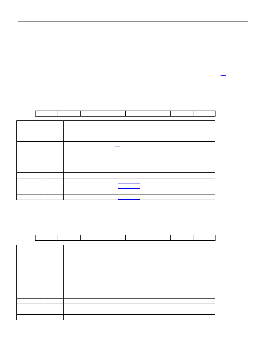
Register Name:
OUTAC
Register Description:
OUTA Control Register
Register Address:
1A Hex
Bit #
7
6
5
4
3
2
1
0
Name
TTLIE
CMII
CMIE
OA4
OA3
OA2
OA1
OA0
NAME
BIT
FUNCTION
TTLIE
7
TTL Input Enable. When this bit is set, the receiver can accept TTL
positive and negative data at the RTIP and RRING inputs. The data is
clocked in on the falling edge of MCLK.
CMII
6
CMI Invert. See Section 22 for details.
0 = CMI input data not inverted
1 = CMI input data inverted
CMIE
5
CMI Enable. See Section 22 for details.
0 = CMI disabled
1 = CMI enabled
OA4
4
OUTA Control Bit 4. Inverts OUTA output.
OA3
3
OUTA Control Bit 3. See Table 20-1 for details.
OA2
2
OUTA Control Bit 2. See Table 20-1 for details.
OA1
1
OUTA Control Bit 1. See Table 20-1 for details.
OA0
0
OUTA Control Bit 0. See Table 20-1 for details.
Register Name:
OUTBC
Register Description:
OUTB Control Register
Register Address:
1B Hex
Bit #
7
6
5
4
3
2
1
0
Name
NRZE
—
OB4
OB3
OB2
OB1
OB0
NAME
BIT
FUNCTION
NRZE
7
NRZ Enable. When this bit is set, the receiver can accept TTL-type NRZ
data at the RTIP input. RRING becomes a clock input.
0 = RTIP and RRING are in normal mode.
1 = RTIP becomes an NRZ TTL-type input and RRING is its associated
clock input. Data at RTIP is clocked in on the falling edge of the clock
present on RRING.
—
6
Unused. Should be set = 0 for proper operation.
—
5
Unused. Should be set = 0 for proper operation.
OB4
4
OUTB Control Bit 4. Inverts OUTB output.
OB3
3
OUTB Control Bit 3
OB2
2
OUTB Control Bit 2
OB1
1
OUTB Control Bit 1
OB0
0
OUTB Control Bit 0
相关PDF资料 |
PDF描述 |
|---|---|
| DS2404B | IC ECONORAM TIMECHIP 5.5V 16SSOP |
| DS2415P+T&R | IC TIME CHIP 1-WIRE 6-TSOC |
| DS2417X/T&R | IC TIMECHIP W/INTRPT 1WIRE CSP |
| DS26502LN+ | IC T1/E1/J1 64KCC ELEMENT 64LQFP |
| DS26503LN+ | IC T1/E1/J1 BITS ELEMENT 64-LQFP |
相关代理商/技术参数 |
参数描述 |
|---|---|
| DS21Q58L+ | 功能描述:网络控制器与处理器 IC Quad E1 Transceiver RoHS:否 制造商:Micrel 产品:Controller Area Network (CAN) 收发器数量: 数据速率: 电源电流(最大值):595 mA 最大工作温度:+ 85 C 安装风格:SMD/SMT 封装 / 箱体:PBGA-400 封装:Tray |
| DS21Q58LN | 功能描述:网络控制器与处理器 IC RoHS:否 制造商:Micrel 产品:Controller Area Network (CAN) 收发器数量: 数据速率: 电源电流(最大值):595 mA 最大工作温度:+ 85 C 安装风格:SMD/SMT 封装 / 箱体:PBGA-400 封装:Tray |
| DS21Q58LN+ | 功能描述:网络控制器与处理器 IC Quad E1 Transceiver RoHS:否 制造商:Micrel 产品:Controller Area Network (CAN) 收发器数量: 数据速率: 电源电流(最大值):595 mA 最大工作温度:+ 85 C 安装风格:SMD/SMT 封装 / 箱体:PBGA-400 封装:Tray |
| DS21Q59 | 制造商:MAXIM 制造商全称:Maxim Integrated Products 功能描述:RELIABILITY REPORT FOR DS21Q59, REV A2 |
| DS21Q59DK | 功能描述:网络开发工具 DS21Q59 Dev Kit RoHS:否 制造商:Rabbit Semiconductor 产品:Development Kits 类型:Ethernet to Wi-Fi Bridges 工具用于评估:RCM6600W 数据速率:20 Mbps, 40 Mbps 接口类型:802.11 b/g, Ethernet 工作电源电压:3.3 V |
发布紧急采购,3分钟左右您将得到回复。