- 您现在的位置:买卖IC网 > PDF目录97868 > DS232AR-N (DALLAS SEMICONDUCTOR) LINE TRANSCEIVER, PDSO16 PDF资料下载
参数资料
| 型号: | DS232AR-N |
| 厂商: | DALLAS SEMICONDUCTOR |
| 元件分类: | Line Driver or Receiver |
| 英文描述: | LINE TRANSCEIVER, PDSO16 |
| 封装: | 0.150 INCH, SOIC-16 |
| 文件页数: | 9/16页 |
| 文件大小: | 224K |
| 代理商: | DS232AR-N |
MAX1501
Highly Integrated, Linear Battery Charger with
Thermal Regulation for Portable Applications
2
Maxim Integrated
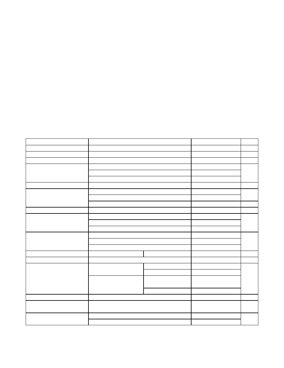
ABSOLUTE MAXIMUM RATINGS
ELECTRICAL CHARACTERISTICS
(VIN = VINP = 5V, VBATT = 3.5V, ACOK = GLED = RLED = TEMP = TMAX/I.C. = FULLI = open, CHGEN = MODE = GND, RSETI = 2.8k
Ω,
CIN = 1F, CBATT = 10F, TA = 0°C to +85°C, unless otherwise noted. Typical values are at TA = +25
°C.)
Stresses beyond those listed under “Absolute Maximum Ratings” may cause permanent damage to the device. These are stress ratings only, and functional
operation of the device at these or any other conditions beyond those indicated in the operational sections of the specifications is not implied. Exposure to
absolute maximum rating conditions for extended periods may affect device reliability.
IN, INP, RLED, GLED to GND ................................-0.3V to +14V
IN to INP ................................................................-0.3V to +0.3V
VL, BATT, SETI, ACOK, MODE, CHGEN, SELV,
FULLI, TMAX/I.C., TEMP to GND .........................-0.3V to +6V
VL to IN...................................................................-14V to +0.3V
Continuous Power Dissipation (TA = +70
°C)
16-Pin 5mm 5mm Thin QFN
(derate 21.3mW/
°C above +70°C).............................1702mW
Operating Temperature Range ...........................-40
°C to +85°C
Junction Temperature ......................................................+150
°C
Storage Temperature Range .............................-65
°C to +150°C
Lead Temperature (soldering, 10s) .................................+300
°C
PARAMETER
CONDITIONS
MIN
TYP
MAX
UNITS
IN, INP Input Voltage
013
V
IN, INP Input Operating Range
4.50
6.25
V
VL Output Voltage
4.5V
≤ VIN ≤ 6.25V, IVL < 250A
2.7
3
3.3
V
VIN - VBATT, rising
40
70
100
VIN - VBATT, falling
30
55
85
ACOK Trip Point
VIN - VBATT, hysteresis
15
mV
ACOK Sink Current
4.5V
≤ VIN ≤ 6.25V, VACOK = 0.6V
75
A
VIN rising
4.05
4.125
4.20
VIN falling
3.9
4.025
4.1
V
Undervoltage Lockout Trip Point
Hysteresis
100
mV
Overvoltage Lockout Trip Point
VIN rising
6.25
6.50
6.75
V
Li+, NiMH/NiCd, and no-battery modes
5
8
Disable mode
1.5
3
IN Input Current
Off mode (VIN = 4V)
0.25
mA
VBATT = 4.3V
45
80
VIN = 0
3
10
BATT Input Current
Disable mode
2
6
A
Leakage into Battery
VIN = VINP = 13V, VBATT = 0
Disable mode
5
A
RMS Charge Current
1.4
A
SELV = VL
4.166
4.2
4.234
Li+ mode
SELV = GND
4.067
4.1
4.133
SELV = VL,
VIN = VINP = 6V
4.85
4.95
5.05
Battery Regulation Voltage
NiMH/NiCd mode
SELV = GND
4.4
4.5
4.6
V
Output Regulation Voltage
No-battery mode
3.700
4.0
4.234
V
BATT Precharge Threshold
Voltage
BATT rising
2.675
2.8
2.925
V
RSETI = 2.8k
Ω
460
500
540
Fast-Charge Current-Loop
System Accuracy
RSETI = 1.75 k
Ω
736
800
864
mA
相关PDF资料 |
PDF描述 |
|---|---|
| DS232AS-N | LINE TRANSCEIVER, PDSO16 |
| DS232AS | LINE TRANSCEIVER, PDSO16 |
| DS232A | LINE TRANSCEIVER, PDIP16 |
| DS2404S-001 | 0 TIMER(S), REAL TIME CLOCK, PDSO16 |
| DS2404B | 0 TIMER(S), REAL TIME CLOCK, PDSO16 |
相关代理商/技术参数 |
参数描述 |
|---|---|
| DS232AR-N/T&R | 制造商:Rochester Electronics LLC 功能描述: 制造商:Maxim Integrated Products 功能描述:IC TXRX DL RS-232 5V IND 16-SOIC |
| DS232AR-N/T&R | 功能描述:RS-232接口集成电路 RoHS:否 制造商:Exar 数据速率:52 Mbps 工作电源电压:5 V 电源电流:300 mA 工作温度范围:- 40 C to + 85 C 安装风格:SMD/SMT 封装 / 箱体:LQFP-100 封装: |
| DS232AR-N+ | 功能描述:RS-232接口集成电路 RoHS:否 制造商:Exar 数据速率:52 Mbps 工作电源电压:5 V 电源电流:300 mA 工作温度范围:- 40 C to + 85 C 安装风格:SMD/SMT 封装 / 箱体:LQFP-100 封装: |
| DS232AR-N+T&R | 制造商:Maxim Integrated Products 功能描述:IC TXRX DUAL RS-232 5V 16-SOIC |
| DS232AR-N+T&R | 功能描述:RS-232接口集成电路 RoHS:否 制造商:Exar 数据速率:52 Mbps 工作电源电压:5 V 电源电流:300 mA 工作温度范围:- 40 C to + 85 C 安装风格:SMD/SMT 封装 / 箱体:LQFP-100 封装: |
发布紧急采购,3分钟左右您将得到回复。