- 您现在的位置:买卖IC网 > PDF目录97868 > DS2423P/T&R (MAXIM INTEGRATED PRODUCTS INC) SPECIALTY MEMORY CIRCUIT, PDSO6 PDF资料下载
参数资料
| 型号: | DS2423P/T&R |
| 厂商: | MAXIM INTEGRATED PRODUCTS INC |
| 元件分类: | Memory IC:Other |
| 英文描述: | SPECIALTY MEMORY CIRCUIT, PDSO6 |
| 封装: | 3.70 X 4 MM, 1.50 MM HEIGHT, TSOC-6 |
| 文件页数: | 11/25页 |
| 文件大小: | 581K |
| 代理商: | DS2423P/T&R |
DS2423
19 of 25
1-WIRE SIGNALING
The DS2423 requires strict protocols to ensure data integrity. The protocol consists of four types of
signaling on one line: Reset Sequence with Reset Pulse and Presence Pulse, Write 0, Write 1 and Read
Data. The bus master initiates all these signals except Presence Pulse. The DS2423 can communicate at
two different speeds, regular speed and Overdrive speed. If not explicitly set into the Overdrive mode, the
DS2423 will communicate at regular speed. While in Overdrive mode the fast timing applies to all
waveforms.
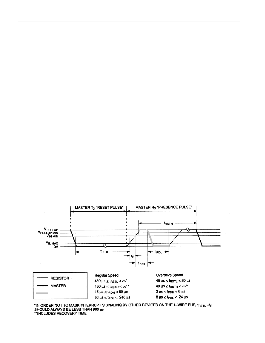
The initialization sequence required to begin any communication with the DS2423 is shown in Figure 10.
A Reset Pulse followed by a Presence Pulse indicates the DS2423 is ready to send or receive data given
the correct ROM command and memory function command. The bus master transmits (TX) a Reset
Pulse (tRSTL, minimum 480 s at regular speed, 48 s at Overdrive speed). The bus master then releases
the line and goes into receive mode (RX). The 1-Wire bus is pulled to a high state via the pullup resistor.
After detecting the rising edge on the data pin, the DS2423 waits (tPDH, 15-60s at regular speed, 2-6s at
Overdrive speed) and then transmits the Presence Pulse (tPDL, 60-240s at regular speed, 8-24s at
Overdrive speed).
A Reset Pulse of 480s or longer will exit the Overdrive mode returning the device to regular speed. If
the DS2423 is in Overdrive mode and the Reset Pulse is no longer than 80s the device will remain in
Overdrive mode.
Read/Write Time Slots
The definitions of write and read time slots are illustrated in Figure 11. All time slots are initiated by the
master driving the data line low. The falling edge of the data line synchronizes the DS2423 to the master
by triggering a delay circuit in the DS2423. During write time slots, the delay circuit determines when the
DS2423 will sample the data line. For a read data time slot, if a “0” is to be transmitted, the delay circuit
determines how long the DS2423 will hold the data line low overriding the 1 generated by the master. If
the data bit is a “1”, the device will leave the read data time slot unchanged.
INITIALIZATION PROCEDURE “RESET AND PRESENCE PULSES” Figure 10
DS2423
Not
Recommended
for
New
Design
相关PDF资料 |
PDF描述 |
|---|---|
| DS2423P | SPECIALTY MEMORY CIRCUIT, PDSO6 |
| DS2423X | SPECIALTY MEMORY CIRCUIT, UUC |
| DS2423 | 4K X 1 STANDARD SRAM, PDSO6 |
| DS2422 | 1K X 1 STANDARD SRAM, PDSO6 |
| DS2430AP | 256 X 1 1-WIRE SERIAL EEPROM, PDSO6 |
相关代理商/技术参数 |
参数描述 |
|---|---|
| DS2423V | 制造商:未知厂家 制造商全称:未知厂家 功能描述:Serial SRAM |
| DS2423X | 功能描述:静态随机存取存储器 RoHS:否 制造商:Cypress Semiconductor 存储容量:16 Mbit 组织:1 M x 16 访问时间:55 ns 电源电压-最大:3.6 V 电源电压-最小:2.2 V 最大工作电流:22 uA 最大工作温度:+ 85 C 最小工作温度:- 40 C 安装风格:SMD/SMT 封装 / 箱体:TSOP-48 封装:Tray |
| DS243 | 制造商:未知厂家 制造商全称:未知厂家 功能描述:Analog IC |
| DS2430 | 制造商:DALLAS 制造商全称:Dallas Semiconductor 功能描述:256-Bit 1-Wire EEPROM |
| DS2430A | 功能描述:电可擦除可编程只读存储器 RoHS:否 制造商:Atmel 存储容量:2 Kbit 组织:256 B x 8 数据保留:100 yr 最大时钟频率:1000 KHz 最大工作电流:6 uA 工作电源电压:1.7 V to 5.5 V 最大工作温度:+ 85 C 安装风格:SMD/SMT 封装 / 箱体:SOIC-8 |
发布紧急采购,3分钟左右您将得到回复。