- 您现在的位置:买卖IC网 > PDF目录1915 > DS2482X-100+T (Maxim Integrated Products)IC MASTER I2C-1WIRE 1CH 9-WLP PDF资料下载
参数资料
| 型号: | DS2482X-100+T |
| 厂商: | Maxim Integrated Products |
| 文件页数: | 7/24页 |
| 文件大小: | 0K |
| 描述: | IC MASTER I2C-1WIRE 1CH 9-WLP |
| 产品培训模块: | Lead (SnPb) Finish for COTS Obsolescence Mitigation Program |
| 标准包装: | 2,500 |
| 控制器类型: | I²C 总线控制器 |
| 接口: | I²C |
| 电源电压: | 2.9 V ~ 5.5 V |
| 电流 - 电源: | 750µA |
| 工作温度: | -40°C ~ 85°C |
| 安装类型: | 表面贴装 |
| 封装/外壳: | 9-WFBGA,WLBGA |
| 供应商设备封装: | 9-WLP |
| 包装: | 带卷 (TR) |
Single-Channel 1-Wire Master
I2C Interface
General Characteristics
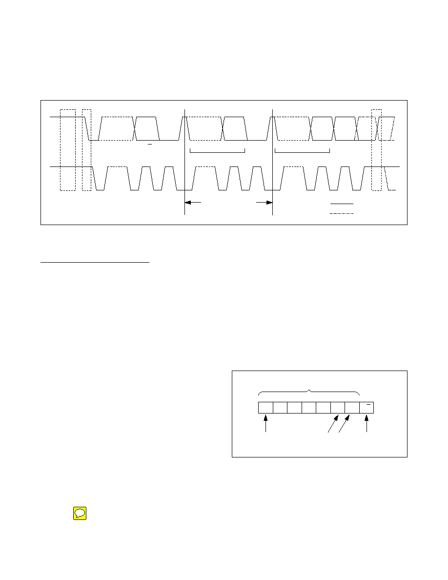
The I2C bus uses a data line (SDA) plus a clock signal
(SCL) for communication. Both SDA and SCL are bidi-
rectional lines, connected to a positive supply voltage
through a pullup resistor. When there is no communica-
tion, both lines are high. The output stages of devices
connected to the bus must have an open drain or open
collector to perform the wired-AND function. Data on
the I2C bus can be transferred at rates of up to
100kbps in standard mode and up to 400kbps in fast
mode. The DS2482-100 works in both modes.
A device that sends data on the bus is defined as a
transmitter, and a device receiving data is defined as a
receiver. The device that controls the communication is
called a master. The devices that are controlled by the
master are slaves. To be individually accessed, each
device must have a slave address that does not conflict
with other devices on the bus.
Data transfers can be initiated only when the bus is not
busy. The master generates the serial clock (SCL), con-
trols the bus access, generates the START and STOP
conditions, and determines the number of data bytes
transferred between START and STOP (Figure 7). Data
is transferred in bytes with the most significant bit being
transmitted first. After each byte follows an acknowledge
bit to allow synchronization between master and slave.
Slave Address
The slave address to which the DS2482-100 responds
is shown in Figure 8. The logic state at the address pins
AD0 and AD1 determines the value of the address bits
A0 and A1. The address pins allow the device to
respond to one of four possible slave addresses. The
slave address is part of the slave address/control byte.
The last bit of the slave address/control byte (R/W)
defines the data direction. When set to 0, subsequent
data flows from master to slave (write access); when
set to 1, data flows from slave to master (read access).
SDA
SCL
IDLE
1–7
8
9
1–7
8
9
1–7
8
9
START
CONDITION
STOP CONDITION
REPEATED START
SLAVE
ADDRESS
R/W
ACK
DATA
ACK/
NACK
DATA
MSB FIRST
MSB
LSB
MSB
LSB
REPEATED IF MORE BYTES
ARE TRANSFERRED
Figure 7. I2C Protocol Overview
Figure 8. DS2482-100 Slave Address
0
A6
MSB
0
A5
1
A4
1
A3
7-BIT SLAVE ADDRESS
0
A2
AD1
A1
AD0
A0
R/W
DETERMINES
READ OR WRITE
AD1, AD0
PIN STATES
DS2482-100
Maxim Integrated
15
相关PDF资料 |
PDF描述 |
|---|---|
| DS2482X-101+T | IC MASTER I2C-1WIRE 1CH 9-WLP |
| DS2483Q+T | IC I2C TO 1WIRE BRIDGE 8TDFN |
| DS2490Y | IC BRIDGE CLIP USB TO 1-W 24SOIC |
| DS26303LN-75+A3 | IC LIU E1/T1/J1 3.3V 144-ELQFP |
| DS26324GNA2+ | IC INTERFACE LINE 16CH 256-CSBGA |
相关代理商/技术参数 |
参数描述 |
|---|---|
| DS2482X-101+T | 功能描述:接口 - 专用 1-Wire Master w/ Sleep Mode RoHS:否 制造商:Texas Instruments 产品类型:1080p60 Image Sensor Receiver 工作电源电压:1.8 V 电源电流:89 mA 最大功率耗散: 最大工作温度:+ 85 C 安装风格:SMD/SMT 封装 / 箱体:BGA-59 |
| DS2482X-101+U | 功能描述:接口 - 专用 SNGL-CH 1-WIRE MASTER w/ SLP MODE RoHS:否 制造商:Texas Instruments 产品类型:1080p60 Image Sensor Receiver 工作电源电压:1.8 V 电源电流:89 mA 最大功率耗散: 最大工作温度:+ 85 C 安装风格:SMD/SMT 封装 / 箱体:BGA-59 |
| DS2483 | 制造商:MAXIM 制造商全称:Maxim Integrated Products 功能描述:Single-Channel 1-Wire Master with Adjustable Timing and Sleep Mode |
| DS2483Q+T | 功能描述:I2C 接口集成电路 Single-Channel 1-Wire Master RoHS:否 制造商:NXP Semiconductors 电源电压-最大:5.5 V 电源电压-最小:2.3 V 最大工作频率:400 KHz 最大工作温度:+ 85 C 封装 / 箱体:TSSOP-16 |
| DS2483Q+U | 功能描述:I2C 接口集成电路 SINGLE-CH 1-WIRE MASTER RoHS:否 制造商:NXP Semiconductors 电源电压-最大:5.5 V 电源电压-最小:2.3 V 最大工作频率:400 KHz 最大工作温度:+ 85 C 封装 / 箱体:TSSOP-16 |
发布紧急采购,3分钟左右您将得到回复。