- 您现在的位置:买卖IC网 > PDF目录9756 > DS26303L-75+ (Maxim Integrated Products)IC LIU E1/T1/J1 3.3V 144-ELQFP PDF资料下载
参数资料
| 型号: | DS26303L-75+ |
| 厂商: | Maxim Integrated Products |
| 文件页数: | 11/101页 |
| 文件大小: | 0K |
| 描述: | IC LIU E1/T1/J1 3.3V 144-ELQFP |
| 产品培训模块: | Lead (SnPb) Finish for COTS Obsolescence Mitigation Program |
| 标准包装: | 15 |
| 类型: | 线路接口装置(LIU) |
| 驱动器/接收器数: | 8/8 |
| 规程: | T1/E1/J1 |
| 电源电压: | 3.135 V ~ 3.465 V |
| 安装类型: | 表面贴装 |
| 封装/外壳: | 144-LQFP 裸露焊盘 |
| 供应商设备封装: | 144-LQFP 裸露焊盘 |
| 包装: | 托盘 |
第1页第2页第3页第4页第5页第6页第7页第8页第9页第10页当前第11页第12页第13页第14页第15页第16页第17页第18页第19页第20页第21页第22页第23页第24页第25页第26页第27页第28页第29页第30页第31页第32页第33页第34页第35页第36页第37页第38页第39页第40页第41页第42页第43页第44页第45页第46页第47页第48页第49页第50页第51页第52页第53页第54页第55页第56页第57页第58页第59页第60页第61页第62页第63页第64页第65页第66页第67页第68页第69页第70页第71页第72页第73页第74页第75页第76页第77页第78页第79页第80页第81页第82页第83页第84页第85页第86页第87页第88页第89页第90页第91页第92页第93页第94页第95页第96页第97页第98页第99页第100页第101页
DS26303: 3.3V, T1/E1/J1, Short-Haul, Octal Line Interface Unit
17 of 101
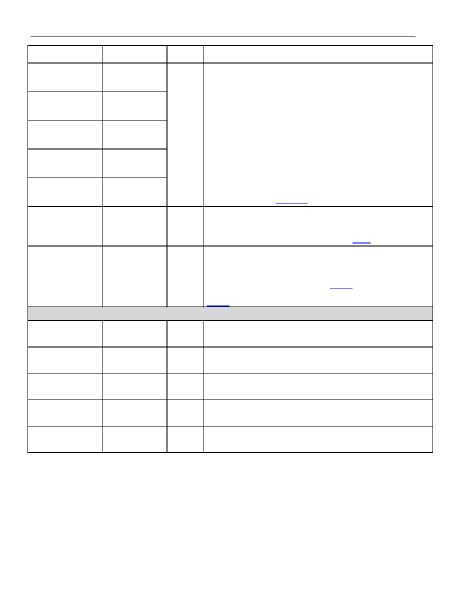
NAME
PIN
TYPE
FUNCTION
A4/RIMPMSB
12
A3/GMC3
13
A2/GMC2
14
A1/GMC1
15
A0/GMC0
16
I
Address Bus 4–0/G.772 Monitoring Control/Rx Impedance
Mode Select
A[4:0]:
These five pins are address pins in parallel host mode. In
serial host mode and multiplexed host mode, these pins should be
grounded.
RIMPMSB:
In hardware mode when this pin is low, the internal
impedance mode is selected, so all RTIP and RING pins require
no external resistance component. When high, external
impedance mode is selected so all RTIP and RING pins require
external resistance.
GMC[3:0]:
In hardware mode, these signal pins are used to select
a transmit line (TTIPn/TRINGn) or receive line (RTIPn/RRINGn)
for nonintrusive monitoring. Receiver 1 is used to monitor
channels 2 to 8 See Table 5-9.
OE
114
I
Output Enable.
If this pin is pulled low, all the transmitter outputs
(TTIPn and TRINGn) are high impedance. Additionally, the user
may use this same pin to turn off all the impedance matching for
the receivers at the same time if register bit GMR.RHPMC is set.
CLKE
115
I
Clock Edge.
When CLKE is high, SDO is valid on the falling edge
of SCLK. When CLKE is low SDO is valid on the rising edge of
SCLK. When CLKE is high, the RCLKn for all the channels is
inverted. This aligns RPOSn/RNEGn on the falling edge of RCLKn
and overrides the settings in register RCLKI. When low,
RPOSn/RNEGn is aligned according to the settings in register
JTAG
JTRSTB
95
I, pullup
JTAG Test Port Reset.
This pin if low resets the JTAG port. If not
used it can be left floating.
JTMS
96
I, pullup
JTAG Test Mode Select.
This pin is clocked on the rising edge of
JTCLK and is used to control the JTAG selection between scan
and test machine control.
JTCLK
97
I
JTAG Test Clock.
The data JTDI and JTMS are clocked on rising
edge of JTCLK and JTDO is clocked out on the falling edge of
JTCLK.
JTDO
98
O,
high-Z
JTAG Test Data Out.
This is the serial output of the JTAG port.
The data is clocked out on the falling edge of JTCLK.
JTDI
99
I, pullup
Test Data Input.
This pin input is the serial data of the JTAG test.
The data on JTDI is clocked on the rising edge of JTCLK. This pin
can be left unconnected.
相关PDF资料 |
PDF描述 |
|---|---|
| MS27474T8B35PA | CONN RCPT 6POS JAM NUT W/PINS |
| MC10E116FNR2G | IC LINE RECEIVER QUINT 28-PLCC |
| DS2450S | IC CONVERTER A/D QUAD 1-W 8-SOIC |
| MS27656T21B11SA | CONN RCPT 11POS WALL MNT W/SCKT |
| 78P2352-IGT/F | IC LIU SDH SONET 2CH 128-LQFP |
相关代理商/技术参数 |
参数描述 |
|---|---|
| DS26303L-75+ | 功能描述:电信线路管理 IC 3.3V E1/T1/J1 Short Haul Octal LIU RoHS:否 制造商:STMicroelectronics 产品:PHY 接口类型:UART 电源电压-最大:18 V 电源电压-最小:8 V 电源电流:30 mA 最大工作温度:+ 85 C 最小工作温度:- 40 C 安装风格:SMD/SMT 封装 / 箱体:VFQFPN-48 封装:Tray |
| DS26303L-75+A3 | 功能描述:电信线路管理 IC 3.3V E1/T1/J1 Short Haul Octal LIU RoHS:否 制造商:STMicroelectronics 产品:PHY 接口类型:UART 电源电压-最大:18 V 电源电压-最小:8 V 电源电流:30 mA 最大工作温度:+ 85 C 最小工作温度:- 40 C 安装风格:SMD/SMT 封装 / 箱体:VFQFPN-48 封装:Tray |
| DS26303L-75A3 | 功能描述:电信线路管理 IC 3.3V E1/T1/J1 Short Haul Octal LIU RoHS:否 制造商:STMicroelectronics 产品:PHY 接口类型:UART 电源电压-最大:18 V 电源电压-最小:8 V 电源电流:30 mA 最大工作温度:+ 85 C 最小工作温度:- 40 C 安装风格:SMD/SMT 封装 / 箱体:VFQFPN-48 封装:Tray |
| DS26303LN-120 | 功能描述:电信线路管理 IC RoHS:否 制造商:STMicroelectronics 产品:PHY 接口类型:UART 电源电压-最大:18 V 电源电压-最小:8 V 电源电流:30 mA 最大工作温度:+ 85 C 最小工作温度:- 40 C 安装风格:SMD/SMT 封装 / 箱体:VFQFPN-48 封装:Tray |
| DS26303LN-120+ | 功能描述:电信线路管理 IC 3.3V E1/T1/J1 Short Haul Octal LIU RoHS:否 制造商:STMicroelectronics 产品:PHY 接口类型:UART 电源电压-最大:18 V 电源电压-最小:8 V 电源电流:30 mA 最大工作温度:+ 85 C 最小工作温度:- 40 C 安装风格:SMD/SMT 封装 / 箱体:VFQFPN-48 封装:Tray |
发布紧急采购,3分钟左右您将得到回复。