参数资料
| 型号: | DS32C35-33IND# |
| 厂商: | Maxim Integrated Products |
| 文件页数: | 22/22页 |
| 文件大小: | 0K |
| 描述: | IC RTC W/TCXO 20-SOIC |
| 产品变化通告: | Product Discontinuation 28/Nov/2011 |
| 标准包装: | 37 |
| 类型: | 时钟/日历 |
| 特点: | 警报器,FRAM,闰年,方波输出,TCXO/晶体 |
| 存储容量: | 8KB |
| 时间格式: | HH:MM:SS(12/24 小时) |
| 数据格式: | YY-MM-DD-dd |
| 接口: | I²C,2 线串口 |
| 电源电压: | 2.7 V ~ 3.63 V |
| 电压 - 电源,电池: | 2.3 V ~ 3.6 V |
| 工作温度: | -40°C ~ 85°C |
| 安装类型: | 表面贴装 |
| 封装/外壳: | 20-SOIC(0.295",7.50mm 宽) |
| 供应商设备封装: | 20-SOIC W |
| 包装: | 管件 |
| 产品目录页面: | 1433 (CN2011-ZH PDF) |
DS32B35/DS32C35
Accurate I2C RTC with Integrated
TCXO/Crystal/FRAM
_____________________________________________________________________
9
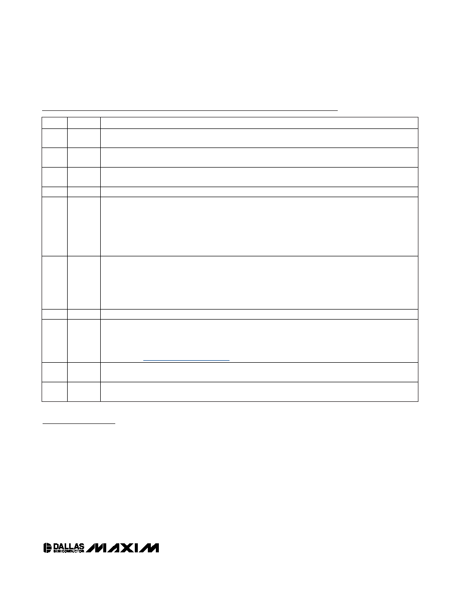
Pin Description
PIN
NAME
FUNCTION
1
WP
Write Protect. When WP is high, the entire FRAM memory array is write protected. When WP is low, all
addresses can be written. This pin is internally pulled down.
2,
7–14
N.C.
No Connection. Must be connected to ground.
3
32kHz
32kHz Output. This open-drain pin requires an external pullup resistor. When enabled, the output operates
on either power supply. It can be left open if not used.
4
VCC
DC Power Pin for Primary Power Supply. This pin should be decoupled using a 0.1μF to 1.0μF capacitor.
5
INT/SQW
Active-Low Interrupt or Square-Wave Output. This open-drain pin requires an external pullup resistor
connected to VCC or another supply of 5.5V or less. It can be left open if not used. This multifunction pin is
determined by the state of the INTCN bit in the Control register (0Eh). When INTCN is set to logic 0, this pin
outputs a square wave and its frequency is determined by the RS2 and RS1 bits. When INTCN is set to logic
1, a match between the timekeeping registers and either of the alarm registers activates the
INT/SQW pin (if
the alarm is enabled). Because the INTCN bit is set to logic 1 when power is first applied, the pin defaults to
an interrupt output with alarms disabled.
6
RST
Active-Low Reset. This pin is an open-drain input/output. It indicates the status of VCC relative to the
VPF specification. As VCC falls below VPF, the
RST pin is driven low. When VCC exceeds VPF, for tRST, the
open-drain pulldown transistor is shut off, and the internal pullup resistor pulls the
RST pin to VCC. The active-
low, open-drain output is combined with a debounced pushbutton input function. This pin can be activated by
a pushbutton reset request. It has an internal 50k
nominal value pullup resistor to VCC. No external pullup
resistors should be connected. If the
EOSC bit is 1, tREC is bypassed and RST immediately goes high.
15, 19
GND
Ground. Must be connected together to ground.
16
VBAT
Backup Power-Supply Input. When using the device with the VBAT input as the primary power source, this
pin should be decoupled using a 0.1μF to 1.0μF low-leakage capacitor. When using the device with the
VBAT input as the backup power source, the capacitor is not required. If VBAT is not used, connect to ground.
The devices are UL recognized to ensure against reverse charging when used with a primary lithium
battery. Go to www.maxim-ic.com/qa/info/ul.
17
SDA
Serial Data Input/Output. This pin is the data input/output for the I2C serial interface. This open-drain pin
requires an external pullup resistor.
18, 20
SCL
Serial Clock Input. These pins are the clock input for the I2C serial interface and are used to synchronize
data movement on the serial interface.
Detailed Description
The DS32B35/DS32C35 accurate RTCs are clock/cal-
endars that include an integrated TCXO, crystal, and a
bank of nonvolatile memory (FRAM) in a single pack-
age. The nonvolatile memory is available in two sizes:
2048 x 8 or 8192 x 8 bits. The integration of the crystal
resonator enhances the long-term accuracy of the
device as well as reduces the piece part count in a
manufacturing line. The devices are available in both
commercial and industrial temperature ranges and is
offered in a 300-mil, 20-pin SO package.
The DS32B35/DS32C35 include a bank of nonvolatile
memory that do not require a backup energy source to
maintain the memory contents. In addition, there are no
read or write cycle limitations. The memory array can
be accessed at maximum cycle rates for the life of the
product with no wear-out mechanisms.
A precision temperature-compensated reference and
comparator circuit monitors the status of VCC and auto-
matically switches to the backup supply when neces-
sary. Other device features include two time-of-day
alarms, a selectable output that provides either an
interrupt or programmable square wave, and a calibrat-
ed 32.768kHz square-wave output. A reset input/output
pin provides a power-on reset. Additionally, the reset
pin is monitored as a pushbutton input for generating a
reset externally. The devices are accessed through an
I2C serial interface.
相关PDF资料 |
PDF描述 |
|---|---|
| DS32C35-33# | IC RTC W/TCXO 20-SOIC |
| AD5259BCPZ10-R7 | IC POT DGTL 10K 256POS 10LFCSP |
| DS32B35-33# | IC RTC W/TCXO 20-SOIC |
| MS3112E22-41S | CONN RCPT 41POS BOX MNT W/SCKT |
| MS27473T22B21SC | CONN PLUG 21POS STRAIGHT W/SCKT |
相关代理商/技术参数 |
参数描述 |
|---|---|
| DS32C35-33IND# | 功能描述:实时时钟 w/Integrated TCXO/Crystal/FRAM RoHS:否 制造商:Microchip Technology 功能:Clock, Calendar. Alarm RTC 总线接口:I2C 日期格式:DW:DM:M:Y 时间格式:HH:MM:SS RTC 存储容量:64 B 电源电压-最大:5.5 V 电源电压-最小:1.8 V 最大工作温度:+ 85 C 最小工作温度: 安装风格:Through Hole 封装 / 箱体:PDIP-8 封装:Tube |
| DS32EL0124 | 制造商:NSC 制造商全称:National Semiconductor 功能描述:125 MHz . 312.5 MHz Deserializer with DDR LVDS Parallel Interface |
| DS32EL0124_0807 | 制造商:NSC 制造商全称:National Semiconductor 功能描述:125 MHz . 312.5 MHz Deserializer with DDR LVDS Parallel Interface |
| DS32EL0124_09 | 制造商:NSC 制造商全称:National Semiconductor 功能描述:125 MHz- 312.5 MHz FPGA-Link Deserializer with DDR LVDS Parallel Interface |
| DS32EL0124SQ | 制造商:NSC 制造商全称:National Semiconductor 功能描述:125 MHz- 312.5 MHz FPGA-Link Deserializer with DDR LVDS Parallel Interface |
发布紧急采购,3分钟左右您将得到回复。