- 您现在的位置:买卖IC网 > PDF目录1916 > DS3905U-020 (Maxim Integrated Products)IC POT NV TRIPLE 128POS 10-USOP PDF资料下载
参数资料
| 型号: | DS3905U-020 |
| 厂商: | Maxim Integrated Products |
| 文件页数: | 10/11页 |
| 文件大小: | 0K |
| 描述: | IC POT NV TRIPLE 128POS 10-USOP |
| 产品培训模块: | Lead (SnPb) Finish for COTS Obsolescence Mitigation Program |
| 标准包装: | 50 |
| 接片: | 128 |
| 电阻(欧姆): | 20k |
| 电路数: | 3 |
| 温度系数: | 标准值 123 ppm/°C |
| 存储器类型: | 非易失 |
| 接口: | I²C(设备位址) |
| 电源电压: | 2.7 V ~ 5.5 V |
| 工作温度: | -40°C ~ 85°C |
| 安装类型: | 表面贴装 |
| 封装/外壳: | 10-TFSOP,10-MSOP(0.118",3.00mm 宽) |
| 供应商设备封装: | 10-µMAX |
| 包装: | 管件 |
DS3904/DS3905
Triple 128-Position Nonvolatile Digital
Variable Resistor/Switch
8
______________________________________________________________________
Bus Reset
After any interruption in protocol, power loss, or system
reset, the following steps reset the DS3904/DS3905:
1)
Clock up to nine cycles.
2)
Look for SDA high in each cycle while SCL is high.
3)
Create a start condition while SDA is high.
Device Addressing
The DS3904/DS3905 must receive an 8-bit device
address byte following a start condition to enable a
specific device for a read or write operation. The
address byte is clocked into the DS3904/DS3905 MSB
to LSB. For the DS3904, the address byte consists of
101000 binary followed by A0 then the R/W bit. If the
R/W bit is high, a read operation is initiated. For the
DS3905, the address byte consists of 1010 binary fol-
lowed by A2, A1, A0 then the R/W bit. If the R/W bit is
low, a write operation is initiated. For a device to
become active, the value of the address bits must be
the same as the hard-wired address pins on the
DS3904/DS3905. Upon a match of written and hard-
wired addresses, the DS3904/DS3905 output a zero for
one clock cycle as an acknowledge. If the address
does not match, the DS3904/DS3905 return to a low-
power mode.
Write Operations
After receiving a matching device address byte with the
R/W bit set low, the device goes into the write mode of
operation. The master must transmit an 8-bit EEPROM
memory address to the device to define the address
where the data is to be written. After the byte has been
received, the DS3904/DS3905 transmit a zero for one
clock cycle to acknowledge that the memory address
has been received. The master must then transmit an 8-
bit data word to be written into this memory address. The
DS3904/DS3905 again transmit a zero for one clock
cycle to acknowledge the receipt of the data byte. At this
point, the master must terminate the write operation with
a stop condition. The DS3904/DS3905 then enter an
internally timed write process tw to the EEPROM memo-
ry. All inputs are disabled during this write cycle.
Acknowledge Polling
Once a EEPROM write is initiated, the part will not
acknowledge until the cycle is complete. Another
option is to wait the maximum write cycle delay before
initiating another write cycle.
Read Operations
After receiving a matching address byte with the R/W bit
set high, the device goes into the read mode of opera-
tion. A read requires a dummy byte write sequence to
load in the register address. Once the device address
and data address bytes are clocked in by the master,
and acknowledged by the DS3904/ DS3905, the master
must generate another start condition (repeated start).
The master now initiates a read by sending the device
address with the R/W bit set high. The DS3904/DS3905
acknowledge the device address and serially clock out
the data byte. The master responds with a NACK and
generates a stop condition afterwards.
See Figures 4 and 5 for command and data byte struc-
tures as well as read and write examples.
2-Wire Serial Port Operation
The 2-wire serial port interface supports a bidirectional
data transmission protocol with device addressing. A
device that sends data on the bus is defined as a trans-
mitter, and a device receiving data as a receiver. The
device that controls the message is called a master. The
devices that are controlled by the master are slaves. The
bus must be controlled by a master device that gener-
ates the SCL, controls the bus access, and generates
the start and stop conditions. The DS3904/DS3905 oper-
ate as slaves on the 2-wire bus. Connections to the bus
are made through SCL and open-drain SDA lines. The
following I/O terminals control the 2-wire serial port: SDA,
SCL, and A0. The DS3905 uses two additional address
pins A1 and A2 to control the 2-wire serial port. Timing
diagrams for the 2-wire serial port can be found in
Figures 2 and 3. Timing information for the 2-wire serial
port is provided in the
AC Electrical Characteristics table
for 2-wire serial communications.
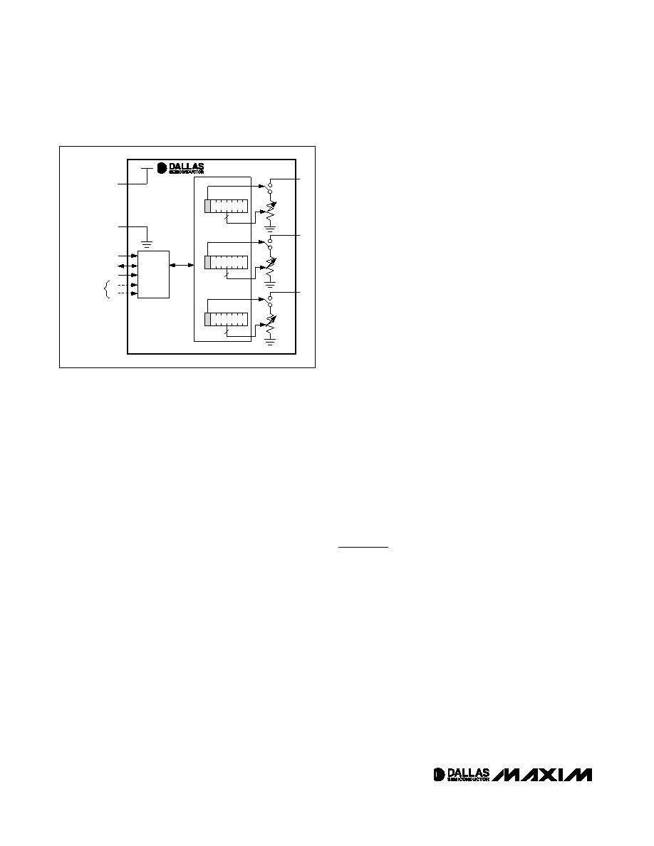
2-WIRE
INTERFACE
RHIZ CONTROL
EEPROM
RES 0
20k
Ω
H0
F8h
MSB
7
LSB
DATA
GND
SCL
SDA
A0
VCC
DS3905
RESISTOR 0
RHIZ CONTROL
RES 1
20k
Ω
OR
10k
Ω
H1
F9h
MSB
LSB
RESISTOR 1
RHIZ CONTROL
RES 2
20k
Ω
H2
FAh
MSB
LSB
RESISTOR 2
7
(DS3905 ONLY)
A1
A2
Figure 1. DS3904/DS3905 Block Diagram
相关PDF资料 |
PDF描述 |
|---|---|
| DS3906U+T&R | IC RESIST VAR TRPL 10USOP |
| DS3908N+T&R | IC POT DUAL DIGITAL 14-TDFN |
| DS3930E | IC POT NV HEX I/O MEM 20-TSSOP |
| DS4301Z-200 | IC POT DIG NV 200K 32POS 8-SOIC |
| DS4520E+TRL | IC I/O EXPANDER I2C 9B 16TSSOP |
相关代理商/技术参数 |
参数描述 |
|---|---|
| DS3905U-020/T&R | 制造商:Maxim Integrated Products 功能描述:TRIPLE NV DIG RES T&R - Tape and Reel |
| DS3905U-020/T&R | 功能描述:数字电位计 IC RoHS:否 制造商:Maxim Integrated 电阻:200 Ohms 温度系数:35 PPM / C 容差:25 % POT 数量:Dual 每 POT 分接头:256 弧刷存储器:Volatile 缓冲刷: 数字接口:Serial (3-Wire, SPI) 描述/功能:Dual Volatile Low Voltage Linear Taper Digital Potentiometer 工作电源电压:1.7 V to 5.5 V 电源电流:27 uA 最大工作温度:+ 125 C 安装风格:SMD/SMT 封装 / 箱体:TQFN-16 封装:Reel |
| DS3905U-020+ | 功能描述:数字电位计 IC Triple 128-Position Nonvolatile RoHS:否 制造商:Maxim Integrated 电阻:200 Ohms 温度系数:35 PPM / C 容差:25 % POT 数量:Dual 每 POT 分接头:256 弧刷存储器:Volatile 缓冲刷: 数字接口:Serial (3-Wire, SPI) 描述/功能:Dual Volatile Low Voltage Linear Taper Digital Potentiometer 工作电源电压:1.7 V to 5.5 V 电源电流:27 uA 最大工作温度:+ 125 C 安装风格:SMD/SMT 封装 / 箱体:TQFN-16 封装:Reel |
| DS3905U-020+T&R | 制造商:Maxim Integrated Products 功能描述:DGTL POTENTIOMETER 128POS 20KOHM TRIPLE 10USOP - Tape and Reel 制造商:Maxim Integrated Products 功能描述:IC POT NV TRIPLE 128POS 10-USOP 制造商:Maxim Integrated Products 功能描述:Digital Potentiometer ICs Triple 128-Position Nonvolatile |
| DS3905U-020+T&R | 功能描述:数字电位计 IC Triple 128-Position Nonvolatile RoHS:否 制造商:Maxim Integrated 电阻:200 Ohms 温度系数:35 PPM / C 容差:25 % POT 数量:Dual 每 POT 分接头:256 弧刷存储器:Volatile 缓冲刷: 数字接口:Serial (3-Wire, SPI) 描述/功能:Dual Volatile Low Voltage Linear Taper Digital Potentiometer 工作电源电压:1.7 V to 5.5 V 电源电流:27 uA 最大工作温度:+ 125 C 安装风格:SMD/SMT 封装 / 箱体:TQFN-16 封装:Reel |
发布紧急采购,3分钟左右您将得到回复。