- 您现在的位置:买卖IC网 > PDF目录1916 > DS5002FMN-16 (Maxim Integrated Products)IC MPU SECURE 16MHZ IND 80-TQFP PDF资料下载
参数资料
| 型号: | DS5002FMN-16 |
| 厂商: | Maxim Integrated Products |
| 文件页数: | 3/25页 |
| 文件大小: | 0K |
| 描述: | IC MPU SECURE 16MHZ IND 80-TQFP |
| 产品培训模块: | Lead (SnPb) Finish for COTS Obsolescence Mitigation Program |
| 标准包装: | 66 |
| 系列: | DS500x |
| 核心处理器: | 8051 |
| 芯体尺寸: | 8-位 |
| 速度: | 16MHz |
| 连通性: | EBI/EMI,SIO,UART/USART |
| 外围设备: | 电源故障复位,WDT |
| 输入/输出数: | 32 |
| 程序存储器类型: | SRAM |
| RAM 容量: | 128 x 8 |
| 电压 - 电源 (Vcc/Vdd): | 4.5 V ~ 5.5 V |
| 振荡器型: | 外部 |
| 工作温度: | -40°C ~ 85°C |
| 封装/外壳: | 80-BQFP |
| 包装: | 托盘 |
DS5002FP Secure Microprocessor Chip
11 of 25
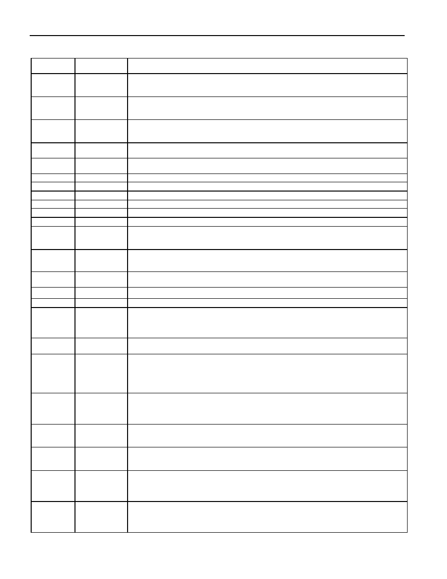
PIN DESCRIPTION
PIN
NAME
FUNCTION
11, 9, 7, 5,
1, 79, 77,
75
P0.0–P0.7
General-Purpose I/O Port 0. This port is open-drain and cannot drive a logic 1. It requires
external pullups. Port 0 is also the multiplexed expanded address/data bus. When used in
this mode, it does not require pullups.
15, 17, 19,
21, 25, 27,
29, 31
P1.0–P1.7
General-Purpose I/O Port 1
49, 50, 51,
56, 58, 60,
64, 66
P2.0–P2.7
General-Purpose I/O Port 2. Also serves as the MSB of the expanded address bus.
36
P3.0/RXD
General-Purpose I/O Port Pin 3.0. Also serves as the receive signal for the on-board UART.
This pin should not be connected directly to a PC COM port.
38
P3.1/TXD
General-Purpose I/O Port Pin 3.1. Also serves as the transmit signal for the on-board
UART. This pin should not be connected directly to a PC COM port.
39
P3.2/
INT0
General-Purpose I/O Port Pin 3.2. Also serves as the active-low external interrupt 0.
40
P3.3/
INT1
General-Purpose I/O Port Pin 3.3. Also serves as the active-low external interrupt 1.
41
P3.4/T0
General-Purpose I/O Port Pin 3.4. Also serves as the timer 0 input.
44
P3.5/T1
General-Purpose I/O Port Pin 3.5. Also serves as the timer 1 input.
45
P3.6/
WR
General-Purpose I/O Port Pin. Also serves as the write strobe for Expanded bus operation.
46
P3.7/
RD
General-Purpose I/O Port Pin. Also serves as the read strobe for Expanded bus operation.
34
RST
Active-High Reset Input. A logic 1 applied to this pin activates a reset state. This pin is
pulled down internally so this pin can be left unconnected if not used. An RC power-on reset
circuit is not needed and is not recommended.
70
ALE
Address Latch Enable. Used to demultiplex the multiplexed expanded address/data bus on
port 0. This pin is normally connected to the clock input on a ’373 type transparent latch.
47, 48
XTAL2, XTAL1
Crystal Connections. Used to connect an external crystal to the internal oscillator. XTAL1 is
the input to an inverting amplifier and XTAL2 is the output.
52
GND
Logic Ground
13
VCC
Power Supply, +5V
12
VCCO
VCC Output. This is switched between VCC and VLI by internal circuits based on the level of
VCC. When power is above the lithium input, power is drawn from VCC. The lithium cell
remains isolated from a load. When VCC is below VLI, the VCCO switches to the VLI source.
VCCO should be connected to the VCC pin of an SRAM.
54
VLI
Lithium Voltage Input. Connect to a lithium cell greater than VLIMIN and no greater than
VLIMAX as shown in the electrical specifications. Nominal value is +3V.
16, 8, 18,
80, 76, 4, 6,
20, 24, 26,
28, 30, 33,
35, 37
BA14–BA0
Byte-Wide Address Bus Bits 14–0. This bus is combined with the nonmultiplexed data bus
(BD7–BD0) to access NV SRAM. Decoding is performed using
CE1 to CE4. Therefore, BA15
is not actually needed. Read/write access is controlled by R/
W. BA14–0 connect directly to an
8k, 32k, or 128k SRAM. If an 8k RAM is used, BA13 and BA14 are unconnected. If a 128k
SRAM is used, the micro converts
CE2 and CE3 to serve as A16 and A15, respectively.
71, 69, 67,
65, 61, 59,
57, 55
BD7–BD0
Byte-Wide Data Bus Bits 7–0. This 8-bit bidirectional bus is combined with the
nonmultiplexed address bus (BA14–BA0) to access NV SRAM. Decoding is performed on
CE1 and CE2. Read/write access is controlled by R/W. D7–D0 connect directly to an SRAM,
and optionally to a real-time clock or other peripheral.
10
R/
W
Read/Write (Active Low). This signal provides the write enable to the SRAMs on the byte-
wide bus. It is controlled by the memory map and partition. The blocks selected as program
(ROM) are write-protected.
74
CE1
Active-Low Chip Enable 1. This is the primary decoded chip enable for memory access on
the byte-wide bus. It connects to the chip-enable input of one SRAM.
CE1 is lithium-backed.
It remains in a logic-high inactive state when VCC falls below VLI.
2
CE2
Active-Low Chip Enable 2. This chip enable is provided to access a second 32k block of
memory. It connects to the chip-enable input of one SRAM. When MSEL = 0, the micro
converts
CE2 into A16 for a 128k x 8 SRAM. CE2 is lithium-backed and remains at a logic
high when VCC falls below VLI.
63
CE3
Active-Low Chip Enable 3. This chip enable is provided to access a third 32k block of
memory. It connects to the chip enable input of one SRAM. When MSEL = 0, the micro
converts
CE3 into A15 for a 128k x 8 SRAM. CE3 is lithium-backed and remains at a logic
high when VCC falls below VLI.
相关PDF资料 |
PDF描述 |
|---|---|
| DS72612RP80FPV | IC SUPERH MPU ROMLESS 176LQFP |
| DS8007-ENG+ | IC SMRT CARD READER INTFC 48LQFP |
| DS8007A-EAG+ | IC INTERFACE SMART CARD 48-LQFP |
| DS8023-RRX+ | IC INTERFACE SMART CARD 28-SOIC |
| DS80C310-ECG | IC MCU HI SPEED 25MHZ 44-TQFP |
相关代理商/技术参数 |
参数描述 |
|---|---|
| DS5002FMN-16+ | 功能描述:微处理器 - MPU Soft MCU Chip RoHS:否 制造商:Atmel 处理器系列:SAMA5D31 核心:ARM Cortex A5 数据总线宽度:32 bit 最大时钟频率:536 MHz 程序存储器大小:32 KB 数据 RAM 大小:128 KB 接口类型:CAN, Ethernet, LIN, SPI,TWI, UART, USB 工作电源电压:1.8 V to 3.3 V 最大工作温度:+ 85 C 安装风格:SMD/SMT 封装 / 箱体:FBGA-324 |
| DS5002FP | 制造商:DALLAS 制造商全称:Dallas Semiconductor 功能描述:Secure Microprocessor Chip |
| DS5002FP/C01 | 功能描述:微处理器 - MPU RoHS:否 制造商:Atmel 处理器系列:SAMA5D31 核心:ARM Cortex A5 数据总线宽度:32 bit 最大时钟频率:536 MHz 程序存储器大小:32 KB 数据 RAM 大小:128 KB 接口类型:CAN, Ethernet, LIN, SPI,TWI, UART, USB 工作电源电压:1.8 V to 3.3 V 最大工作温度:+ 85 C 安装风格:SMD/SMT 封装 / 箱体:FBGA-324 |
| DS5002FP_06 | 制造商:DALLAS 制造商全称:Dallas Semiconductor 功能描述:Secure Microprocessor Chip |
| DS5002FP_1 | 制造商:DALLAS 制造商全称:Dallas Semiconductor 功能描述:Secure Microprocessor Chip |
发布紧急采购,3分钟左右您将得到回复。