- 您现在的位置:买卖IC网 > PDF目录97870 > DS80C390-FCR (MAXIM INTEGRATED PRODUCTS INC) 8-BIT, MROM, 100 MHz, MICROCONTROLLER, PQFP64 PDF资料下载
参数资料
| 型号: | DS80C390-FCR |
| 厂商: | MAXIM INTEGRATED PRODUCTS INC |
| 元件分类: | Microcontroller |
| 英文描述: | 8-BIT, MROM, 100 MHz, MICROCONTROLLER, PQFP64 |
| 封装: | LQFP-64 |
| 文件页数: | 30/54页 |
| 文件大小: | 2030K |
| 代理商: | DS80C390-FCR |
第1页第2页第3页第4页第5页第6页第7页第8页第9页第10页第11页第12页第13页第14页第15页第16页第17页第18页第19页第20页第21页第22页第23页第24页第25页第26页第27页第28页第29页当前第30页第31页第32页第33页第34页第35页第36页第37页第38页第39页第40页第41页第42页第43页第44页第45页第46页第47页第48页第49页第50页第51页第52页第53页第54页
DS80C390 Dual CAN High-Speed Microprocessor
36 of 54
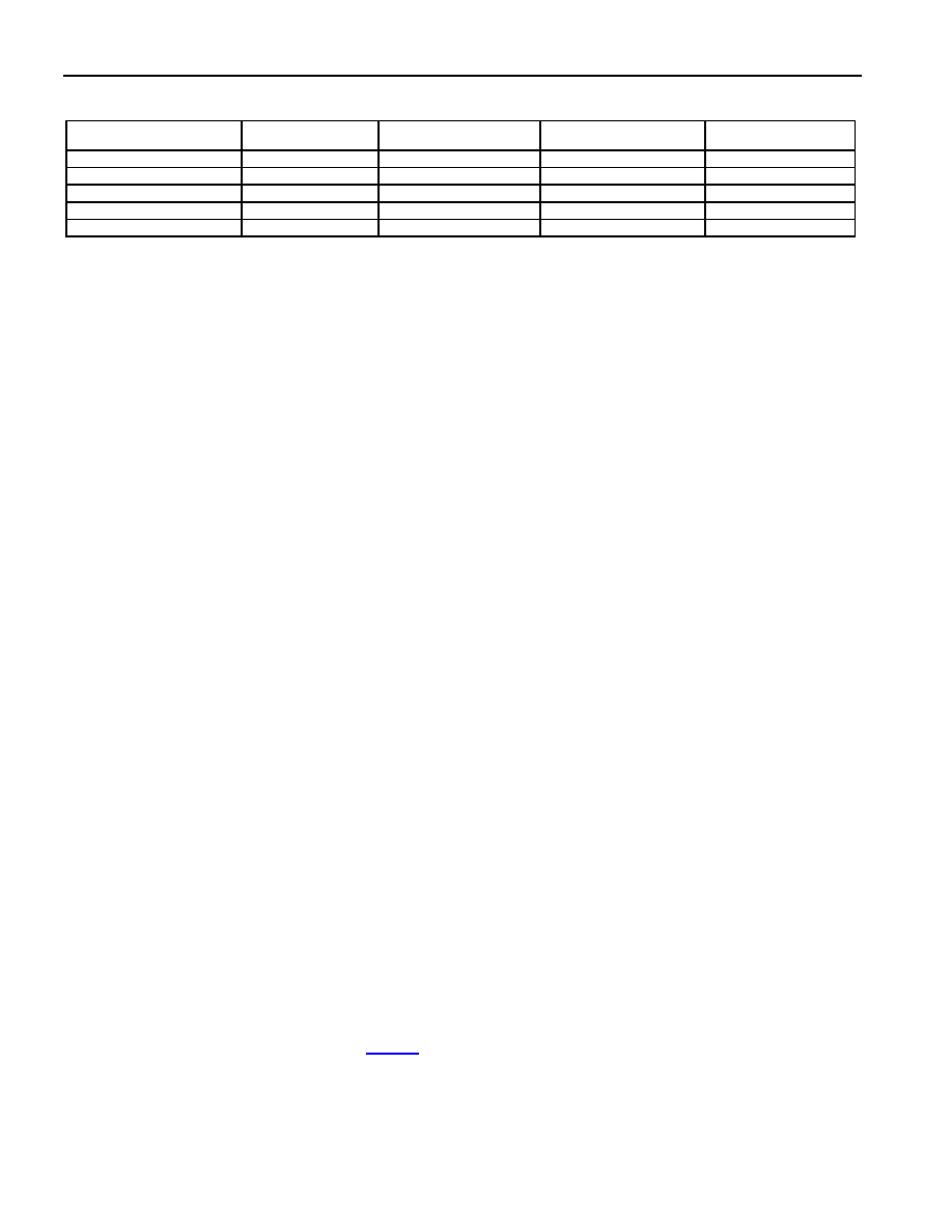
Table 8. Program Memory Chip-Enable Boundaries
P4CNT.5–3
CE0
CE1
CE2
CE3
000
0h–7FFFh
8000h–FFFFh
10000h–17FFFh
18000h–1FFFFh
100
0h–1FFFFh
20000h–3FFFFh
40000h–5FFFFh
60000h–7FFFFh
101
0h–3FFFFh
40000h–7FFFFh
80000h–BFFFFh
C0000h–FFFFFh
110
0h–7FFFFh
80000h–FFFFFh
100000h–17FFFFh
180000h–1FFFFFh
111(default)
0–FFFFFh
100000h–1FFFFFh
200000h–2FFFFFh
300000h–3FFFFFh
The DS80C390 incorporates a feature allowing PCE and CE signals to be combined. This is useful when
incorporating modifiable code memory as part of a bootstrap loader or for in-system reprogrammability. Setting the
PDCE3–0 (MCON.3–0) bits causes the corresponding chip-enable signal to function for both MOVC and MOVX
operations. Write access to combined program and data memory blocks is controlled by the
WR signal, and read
access is controlled by the
PSEN signal. This feature is especially useful if the design achieves in-system
reprogrammability via external flash memory, in which a single device is accessed through both MOVC instructions
(program fetch) and MOVX write operations (updates to code memory). In this case, the internal SRAM is placed in
the program/data configuration and loaded with a small bootstrap loader program stored in the external flash
memory. The device then executes the internal bootstrap loader routine to modify/update the program memory
located in the external flash memory.
STRETCH MEMORY CYCLES
The DS80C390 allows user-application software to select the number of machine cycles it takes to execute a
MOVX instruction, allowing access to both fast and slow off-chip data memory and/or peripherals without glue
logic. High-speed systems often include memory-mapped peripherals such as LCDs or UARTs with slow access
times, so it may not be necessary or desirable to access external devices at full speed. The microprocessor can
perform a MOVX instruction in as little as two machine cycles or as many as twelve machine cycles. Accesses to
internal MOVX SRAM always use two cycles. Note that stretch cycle settings affect external MOVX memory
operations only and that there is no way to slow the accesses to program memory other than to use a slower
crystal (or external clock).
External MOVX timing is governed by the selection of 0 to 7 stretch cycles, controlled by the MD2–MD0 SFR bits in
the clock-control register (CKCON.2–0). A stretch of zero results in a 2-machine cycle MOVX instruction. A stretch
of seven results in a MOVX of 12 machine cycles. Software can dynamically change the stretch value depending
on the particular memory or peripheral being accessed. The default of one stretch cycle allows the use of
commonly available SRAMs without dramatically lengthening the memory access times.
Stretch cycle settings affect external MOVX timing in three gradations. Changing the stretch value from 0 to 1 adds
an additional clock cycle each to the data setup and hold times. When a stretch value of 4 or above is selected, the
interface timing changes dramatically to allow for very slow peripherals. First, the ALE signal is lengthened by 1
machine cycle. This increases the address setup time into the peripheral by this amount. Next, the address is held
on the bus for one additional machine cycle increasing the address hold time by this amount. The
WR and RD
signals are then lengthened by a machine cycle. Finally, during a MOVX write the data is held on the bus for one
additional machine cycle, thereby increasing the data hold time by this amount. For every stretch value greater
than 4, the setup and hold times remain constant, and only the width of the read or write signal is increased. These
three gradations are reflected in the AC Electrical Characteristics, where the eight MOVX timing specifications are
represented by only three timing diagrams.
The reset default of one stretch cycle results in a three-cycle MOVX for any external access. Therefore, the default
off-chip RAM access is not at full speed. This is a convenience to existing designs that use slower RAM. When
maximum speed is desired, software should select a stretch value of zero. When using very slow RAM or
peripherals, the application software can select a larger stretch value.
The specific timing of MOVX instructions as a function of stretch settings is provided in the Electrical Specifications
section of this data sheet. As an example, Table 9 shows the read and write strobe widths corresponding to each
stretch value.
相关PDF资料 |
PDF描述 |
|---|---|
| DS80C390-QCR | 8-BIT, MROM, 100 MHz, MICROCONTROLLER, PQCC68 |
| DS80C390-QNR | 8-BIT, 40 MHz, MICROCONTROLLER, PQCC68 |
| DS80C390-FNR | 8-BIT, 40 MHz, MICROCONTROLLER, PQFP64 |
| DS80CH11 | 8-BIT, MICROCONTROLLER, PQFP128 |
| DS83C530-ENL | 8-BIT, OTPROM, 33 MHz, MICROCONTROLLER, PQFP52 |
相关代理商/技术参数 |
参数描述 |
|---|---|
| DS80C390-FCR+ | 功能描述:8位微控制器 -MCU Dual CAN High-Speed RoHS:否 制造商:Silicon Labs 核心:8051 处理器系列:C8051F39x 数据总线宽度:8 bit 最大时钟频率:50 MHz 程序存储器大小:16 KB 数据 RAM 大小:1 KB 片上 ADC:Yes 工作电源电压:1.8 V to 3.6 V 工作温度范围:- 40 C to + 105 C 封装 / 箱体:QFN-20 安装风格:SMD/SMT |
| DS80C390-FNR | 功能描述:8位微控制器 -MCU Dual CAN High-Speed RoHS:否 制造商:Silicon Labs 核心:8051 处理器系列:C8051F39x 数据总线宽度:8 bit 最大时钟频率:50 MHz 程序存储器大小:16 KB 数据 RAM 大小:1 KB 片上 ADC:Yes 工作电源电压:1.8 V to 3.6 V 工作温度范围:- 40 C to + 105 C 封装 / 箱体:QFN-20 安装风格:SMD/SMT |
| DS80C390-FNR+ | 功能描述:8位微控制器 -MCU Dual CAN High-Speed RoHS:否 制造商:Silicon Labs 核心:8051 处理器系列:C8051F39x 数据总线宽度:8 bit 最大时钟频率:50 MHz 程序存储器大小:16 KB 数据 RAM 大小:1 KB 片上 ADC:Yes 工作电源电压:1.8 V to 3.6 V 工作温度范围:- 40 C to + 105 C 封装 / 箱体:QFN-20 安装风格:SMD/SMT |
| DS80C390-QCR | 功能描述:8位微控制器 -MCU Dual CAN High-Speed RoHS:否 制造商:Silicon Labs 核心:8051 处理器系列:C8051F39x 数据总线宽度:8 bit 最大时钟频率:50 MHz 程序存储器大小:16 KB 数据 RAM 大小:1 KB 片上 ADC:Yes 工作电源电压:1.8 V to 3.6 V 工作温度范围:- 40 C to + 105 C 封装 / 箱体:QFN-20 安装风格:SMD/SMT |
| DS80C390-QCR+ | 功能描述:8位微控制器 -MCU Dual CAN High-Speed RoHS:否 制造商:Silicon Labs 核心:8051 处理器系列:C8051F39x 数据总线宽度:8 bit 最大时钟频率:50 MHz 程序存储器大小:16 KB 数据 RAM 大小:1 KB 片上 ADC:Yes 工作电源电压:1.8 V to 3.6 V 工作温度范围:- 40 C to + 105 C 封装 / 箱体:QFN-20 安装风格:SMD/SMT |
发布紧急采购,3分钟左右您将得到回复。