- 您现在的位置:买卖IC网 > PDF目录11784 > DS89C450-ENL+ (Maxim Integrated Products)IC MCU FLASH 64KB 33MHZ 44-TQFP PDF资料下载
参数资料
| 型号: | DS89C450-ENL+ |
| 厂商: | Maxim Integrated Products |
| 文件页数: | 33/46页 |
| 文件大小: | 0K |
| 描述: | IC MCU FLASH 64KB 33MHZ 44-TQFP |
| 产品培训模块: | Lead (SnPb) Finish for COTS Obsolescence Mitigation Program |
| 标准包装: | 160 |
| 系列: | 89C |
| 核心处理器: | 8051 |
| 芯体尺寸: | 8-位 |
| 速度: | 33MHz |
| 连通性: | EBI/EMI,SIO,UART/USART |
| 外围设备: | 电源故障复位,WDT |
| 输入/输出数: | 32 |
| 程序存储器容量: | 64KB(64K x 8) |
| 程序存储器类型: | 闪存 |
| RAM 容量: | 1K x 8 |
| 电压 - 电源 (Vcc/Vdd): | 4.5 V ~ 5.5 V |
| 振荡器型: | 外部 |
| 工作温度: | -40°C ~ 85°C |
| 封装/外壳: | 44-TQFP |
| 包装: | 托盘 |
| 产品目录页面: | 703 (CN2011-ZH PDF) |
第1页第2页第3页第4页第5页第6页第7页第8页第9页第10页第11页第12页第13页第14页第15页第16页第17页第18页第19页第20页第21页第22页第23页第24页第25页第26页第27页第28页第29页第30页第31页第32页当前第33页第34页第35页第36页第37页第38页第39页第40页第41页第42页第43页第44页第45页第46页
DS89C430/DS89C450 Ultra-High-Speed Flash Microcontrollers
39 of 46
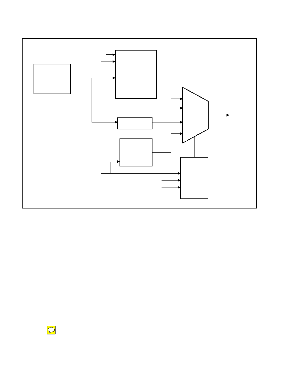
Figure 14. System Clock Sources
4X/2X
CTM
CRYSTAL
OSCILLATOR
DIVIDE 1024
RING
OSCILLATOR
CLOCK
MULTIPLIER
CD0
CD1
SELECTOR
RING
ENABLE
MUX
SYSTEM
CLOCK
Bandgap-Monitored Interrupt and Reset Generation
The power monitor in the DS89C430 monitors the VCC pin in relation to the on-chip bandgap voltage reference.
Whenever VCC falls below VPFW, an interrupt is generated if the corresponding power-fail interrupt-enable bit EPFI
(WDCON.5) is set, causing the device to vector to address 33h. The power-fail interrupt status bit PFI (WDCON.4)
is set any time VCC transitions below VPFW, and can only be cleared by software once set. Similarly, as VCC falls
below VRST, a reset is issued internally to halt program execution. Following power-up, a power-on reset initiates a
power-on reset timeout before starting program execution. When VCC is first applied to the DS89C430, the
processor is held in reset until VCC > VRST and a delay of 65,536 oscillator cycles has elapsed, to ensure that power
is within tolerance and the clock source has had time to stabilize. Once the reset timeout period has elapsed, the
reset condition is removed automatically and software execution begins at the reset vector location of 0000h. The
power-on reset flag POR (WDCON.6) is set to logic 1 to indicate a power-on reset has occurred, and can only be
cleared by software.
When the DS89C430 enters stop mode, the bandgap, reset comparator, and power-fail interrupt comparator are
automatically disabled to conserve power if the BGS (EXIF.0) bit is set to logic 0. This is the lowest power mode. If
BGS is set to logic 1, the bandgap reference, reset comparator, and the power-fail comparator are powered up,
although in a mode that reduces their power consumption.
相关PDF资料 |
PDF描述 |
|---|---|
| VE-B43-IW-F3 | CONVERTER MOD DC/DC 24V 100W |
| DS89C450-MNL+ | IC MCU FLASH 64KB 33MHZ 40-DIP |
| VE-B43-IW-F2 | CONVERTER MOD DC/DC 24V 100W |
| DS89C450-QNL+ | IC MCU FLASH 64KB 33MHZ 44-PLCC |
| VE-B43-IW-F1 | CONVERTER MOD DC/DC 24V 100W |
相关代理商/技术参数 |
参数描述 |
|---|---|
| DS89C450-ENL+ | 功能描述:8位微控制器 -MCU Ultra-High-Speed Flash MCU RoHS:否 制造商:Silicon Labs 核心:8051 处理器系列:C8051F39x 数据总线宽度:8 bit 最大时钟频率:50 MHz 程序存储器大小:16 KB 数据 RAM 大小:1 KB 片上 ADC:Yes 工作电源电压:1.8 V to 3.6 V 工作温度范围:- 40 C to + 105 C 封装 / 箱体:QFN-20 安装风格:SMD/SMT |
| DS89C450-K00 | 功能描述:开发板和工具包 - 8051 RoHS:否 制造商:Silicon Labs 产品:Development Kits 工具用于评估:C8051F960, Si7005 核心: 接口类型:USB 工作电源电压: |
| DS89C450-KIT# | 功能描述:开发板和工具包 - 8051 Ultra-High-Speed Flash MCU RoHS:否 制造商:Silicon Labs 产品:Development Kits 工具用于评估:C8051F960, Si7005 核心: 接口类型:USB 工作电源电压: |
| DS89C450-MNG | 功能描述:8位微控制器 -MCU Ultra-High-Speed Flash MCU RoHS:否 制造商:Silicon Labs 核心:8051 处理器系列:C8051F39x 数据总线宽度:8 bit 最大时钟频率:50 MHz 程序存储器大小:16 KB 数据 RAM 大小:1 KB 片上 ADC:Yes 工作电源电压:1.8 V to 3.6 V 工作温度范围:- 40 C to + 105 C 封装 / 箱体:QFN-20 安装风格:SMD/SMT |
| DS89C450-MNG+ | 功能描述:8位微控制器 -MCU Ultra-High-Speed Flash MCU RoHS:否 制造商:Silicon Labs 核心:8051 处理器系列:C8051F39x 数据总线宽度:8 bit 最大时钟频率:50 MHz 程序存储器大小:16 KB 数据 RAM 大小:1 KB 片上 ADC:Yes 工作电源电压:1.8 V to 3.6 V 工作温度范围:- 40 C to + 105 C 封装 / 箱体:QFN-20 安装风格:SMD/SMT |
发布紧急采购,3分钟左右您将得到回复。