- 您现在的位置:买卖IC网 > PDF目录11784 > DS89C450-ENL+ (Maxim Integrated Products)IC MCU FLASH 64KB 33MHZ 44-TQFP PDF资料下载
参数资料
| 型号: | DS89C450-ENL+ |
| 厂商: | Maxim Integrated Products |
| 文件页数: | 4/46页 |
| 文件大小: | 0K |
| 描述: | IC MCU FLASH 64KB 33MHZ 44-TQFP |
| 产品培训模块: | Lead (SnPb) Finish for COTS Obsolescence Mitigation Program |
| 标准包装: | 160 |
| 系列: | 89C |
| 核心处理器: | 8051 |
| 芯体尺寸: | 8-位 |
| 速度: | 33MHz |
| 连通性: | EBI/EMI,SIO,UART/USART |
| 外围设备: | 电源故障复位,WDT |
| 输入/输出数: | 32 |
| 程序存储器容量: | 64KB(64K x 8) |
| 程序存储器类型: | 闪存 |
| RAM 容量: | 1K x 8 |
| 电压 - 电源 (Vcc/Vdd): | 4.5 V ~ 5.5 V |
| 振荡器型: | 外部 |
| 工作温度: | -40°C ~ 85°C |
| 封装/外壳: | 44-TQFP |
| 包装: | 托盘 |
| 产品目录页面: | 703 (CN2011-ZH PDF) |
第1页第2页第3页当前第4页第5页第6页第7页第8页第9页第10页第11页第12页第13页第14页第15页第16页第17页第18页第19页第20页第21页第22页第23页第24页第25页第26页第27页第28页第29页第30页第31页第32页第33页第34页第35页第36页第37页第38页第39页第40页第41页第42页第43页第44页第45页第46页
DS89C430/DS89C450 Ultra-High-Speed Flash Microcontrollers
12 of 46
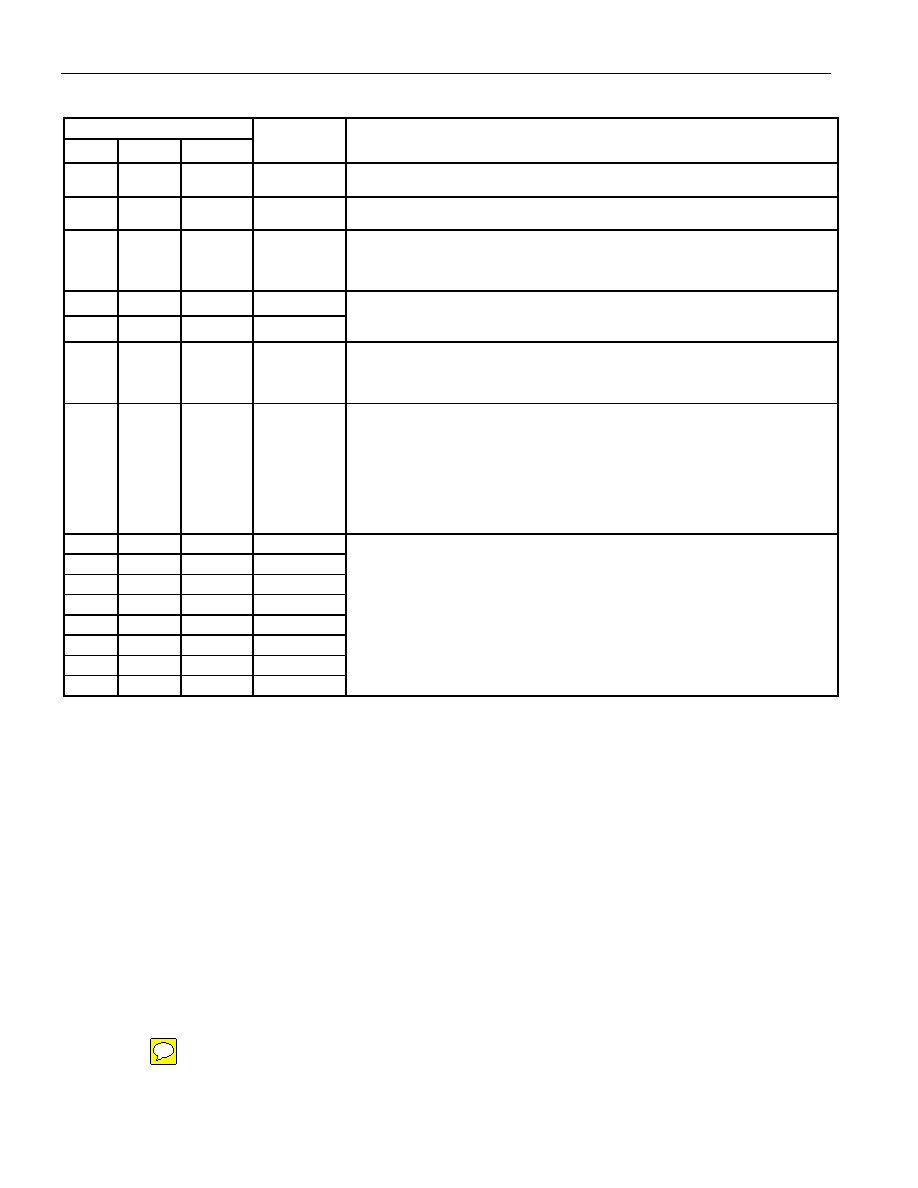
PIN DESCRIPTION
PIN
PDIP
PLCC
TQFP
NAME
FUNCTION
40
12, 44
6, 38
VCC
+5V
20
1, 22, 23,
34
16, 17, 28,
39
GND
Logic Ground
9
10
4
RST
External Reset. The RST input pin is bidirectional and contains a Schmitt Trigger to
recognize external active-high reset inputs. The pin also employs an internal pulldown
resistor to allow for a combination of wire-ORed external reset sources. An RC is not
required for power-up, as the device provides this function internally.
19
21
15
XTAL1
18
20
14
XTAL2
Crystal Oscillators. These pins provide support for fundamental-mode parallel-resonant
AT-cut crystals. XTAL1 also acts as an input if there is an external clock source in place of
a crystal. XTAL2 serves as the output of the crystal amplifier.
29
32
26
PSEN
Program Store Enable. This signal is commonly connected to optional external program
memory as a chip enable. PSEN provides an active-low pulse and is driven high when
external program memory is not being accessed. In one-cycle page mode 1, PSEN
remains low for consecutive page hits.
30
33
27
ALE/PROG
Address Latch Enable. This signal functions as a clock to latch the external address LSB
from the multiplexed address/data bus on Port 0. This signal is commonly connected to the
latch enable of an external 373-family transparent latch. In default mode, ALE has a pulse
width of 1.5 XTAL1 cycles and a period of four XTAL1 cycles. In page mode, the ALE
pulse width is altered according to the page mode selection. In traditional 8051 mode, ALE
is high when using the EMI reduction mode and during a reset condition. ALE can be
enabled by writing ALEON = 1 (PMR.2). Note that ALE operates independently of ALEON
during external memory accesses. As an alternate mode, this pin (PROG) is used to
execute the parallel program function.
39
43
37
P0.0 (AD0)
38
42
36
P0.1 (AD1)
37
41
35
P0.2 (AD2)
36
40
34
P0.3 (AD3)
35
39
33
P0.4 (AD4)
34
38
32
P0.5 (AD5)
33
37
31
P0.6 (AD6)
32
36
30
P0.7 (AD7)
Port 0 (AD0–AD7), I/O. Port 0 is an open-drain, 8-bit, bidirectional I/O port. As an
alternate function, Port 0 can function as the multiplexed address/data bus to access off-
chip memory. During the time when ALE is high, the LSB of a memory address is
presented. When ALE falls to logic 0, the port transitions to a bidirectional data bus. This
bus is used to read external program memory and read/write external RAM or peripherals.
When used as a memory bus, the port provides weak pullups for logic 1 outputs. The reset
condition of port 0 is tri-state. Pullup resistors are required only when using port 0 as an
I/O port.
相关PDF资料 |
PDF描述 |
|---|---|
| VE-B43-IW-F3 | CONVERTER MOD DC/DC 24V 100W |
| DS89C450-MNL+ | IC MCU FLASH 64KB 33MHZ 40-DIP |
| VE-B43-IW-F2 | CONVERTER MOD DC/DC 24V 100W |
| DS89C450-QNL+ | IC MCU FLASH 64KB 33MHZ 44-PLCC |
| VE-B43-IW-F1 | CONVERTER MOD DC/DC 24V 100W |
相关代理商/技术参数 |
参数描述 |
|---|---|
| DS89C450-ENL+ | 功能描述:8位微控制器 -MCU Ultra-High-Speed Flash MCU RoHS:否 制造商:Silicon Labs 核心:8051 处理器系列:C8051F39x 数据总线宽度:8 bit 最大时钟频率:50 MHz 程序存储器大小:16 KB 数据 RAM 大小:1 KB 片上 ADC:Yes 工作电源电压:1.8 V to 3.6 V 工作温度范围:- 40 C to + 105 C 封装 / 箱体:QFN-20 安装风格:SMD/SMT |
| DS89C450-K00 | 功能描述:开发板和工具包 - 8051 RoHS:否 制造商:Silicon Labs 产品:Development Kits 工具用于评估:C8051F960, Si7005 核心: 接口类型:USB 工作电源电压: |
| DS89C450-KIT# | 功能描述:开发板和工具包 - 8051 Ultra-High-Speed Flash MCU RoHS:否 制造商:Silicon Labs 产品:Development Kits 工具用于评估:C8051F960, Si7005 核心: 接口类型:USB 工作电源电压: |
| DS89C450-MNG | 功能描述:8位微控制器 -MCU Ultra-High-Speed Flash MCU RoHS:否 制造商:Silicon Labs 核心:8051 处理器系列:C8051F39x 数据总线宽度:8 bit 最大时钟频率:50 MHz 程序存储器大小:16 KB 数据 RAM 大小:1 KB 片上 ADC:Yes 工作电源电压:1.8 V to 3.6 V 工作温度范围:- 40 C to + 105 C 封装 / 箱体:QFN-20 安装风格:SMD/SMT |
| DS89C450-MNG+ | 功能描述:8位微控制器 -MCU Ultra-High-Speed Flash MCU RoHS:否 制造商:Silicon Labs 核心:8051 处理器系列:C8051F39x 数据总线宽度:8 bit 最大时钟频率:50 MHz 程序存储器大小:16 KB 数据 RAM 大小:1 KB 片上 ADC:Yes 工作电源电压:1.8 V to 3.6 V 工作温度范围:- 40 C to + 105 C 封装 / 箱体:QFN-20 安装风格:SMD/SMT |
发布紧急采购,3分钟左右您将得到回复。