- 您现在的位置:买卖IC网 > PDF目录3793 > DSP56F805FV80 (Freescale Semiconductor)IC DSP 80MHZ 64KB FLASH 144LQFP PDF资料下载
参数资料
| 型号: | DSP56F805FV80 |
| 厂商: | Freescale Semiconductor |
| 文件页数: | 16/56页 |
| 文件大小: | 0K |
| 描述: | IC DSP 80MHZ 64KB FLASH 144LQFP |
| 标准包装: | 60 |
| 系列: | 56F8xx |
| 核心处理器: | 56800 |
| 芯体尺寸: | 16-位 |
| 速度: | 80MHz |
| 连通性: | CAN,EBI/EMI,SCI,SPI |
| 外围设备: | POR,PWM,WDT |
| 输入/输出数: | 32 |
| 程序存储器容量: | 71KB(35.5K x 16) |
| 程序存储器类型: | 闪存 |
| RAM 容量: | 2.5K x 16 |
| 电压 - 电源 (Vcc/Vdd): | 3 V ~ 3.6 V |
| 数据转换器: | A/D 8x12b |
| 振荡器型: | 外部 |
| 工作温度: | -40°C ~ 85°C |
| 封装/外壳: | 144-LQFP |
| 包装: | 托盘 |
第1页第2页第3页第4页第5页第6页第7页第8页第9页第10页第11页第12页第13页第14页第15页当前第16页第17页第18页第19页第20页第21页第22页第23页第24页第25页第26页第27页第28页第29页第30页第31页第32页第33页第34页第35页第36页第37页第38页第39页第40页第41页第42页第43页第44页第45页第46页第47页第48页第49页第50页第51页第52页第53页第54页第55页第56页
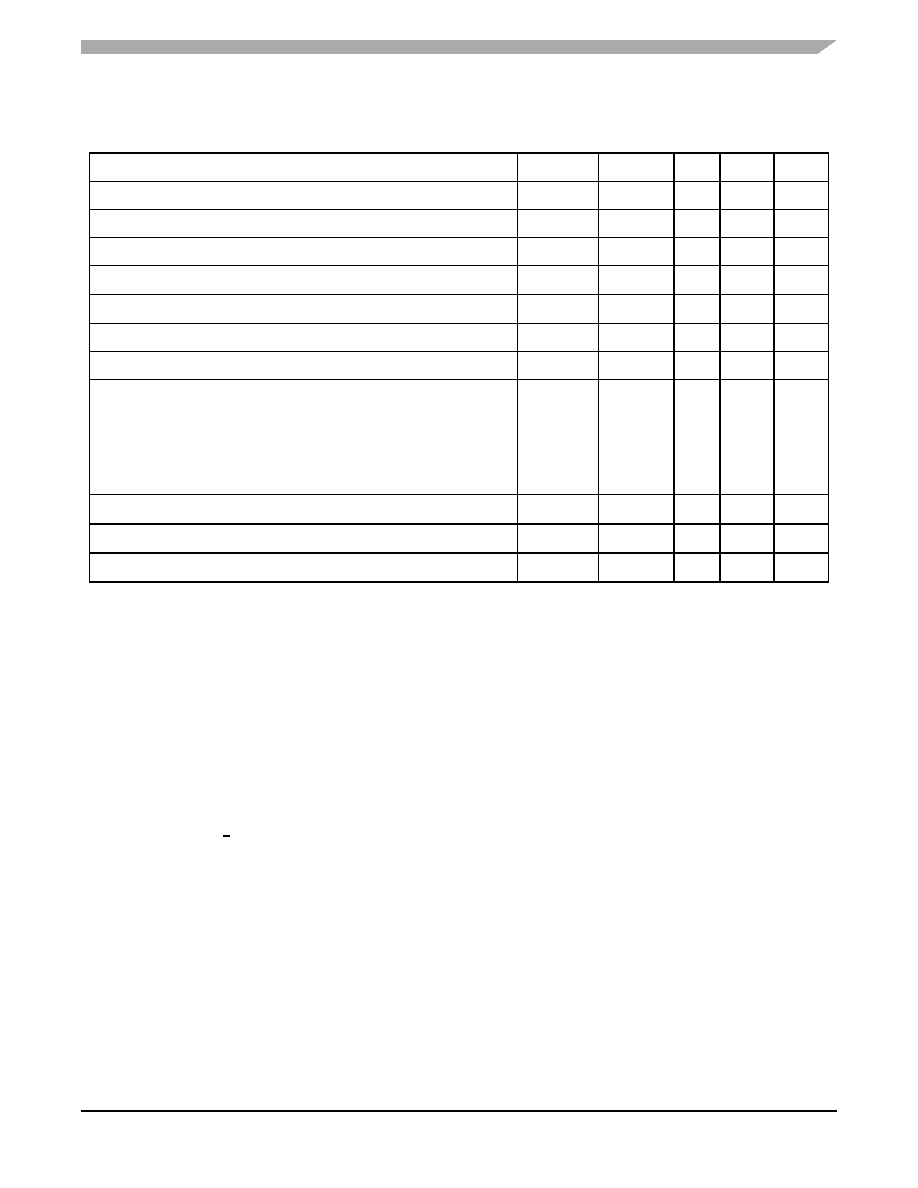
DC Electrical Characteristics
56F805 Technical Data, Rev. 16
Freescale Semiconductor
23
Output Low Voltage (at IOL)
VOL
——
0.4
V
Output source current
IOH
4—
—
mA
Output sink current
IOL
4—
—
mA
PWM pin output source current3
IOHP
10
—
mA
PWM pin output sink current4
IOLP
16
—
mA
Input capacitance
CIN
—8
—
pF
Output capacitance
COUT
—12
—
pF
VDD supply current
IDDT
5
Run 6
—
126
152
mA
Wait7
—
105
129
mA
Stop
—60
84
mA
Low Voltage Interrupt, external power supply8
VEIO
2.4
2.7
3.0
V
Low Voltage Interrupt, internal power supply9
VEIC
2.0
2.2
2.4
V
Power on Reset10
VPOR
—1.7
2.0
V
1.
Schmitt Trigger inputs are: EXTBOOT, IRQA, IRQB, RESET, ISA0-2, FAULTA0-3, ISB0-2, FAULT0B-3, TCS, TCK, TRST, TMS,
TDI, and MSCAN_RX
2.
Analog inputs are: ANA[0:7], XTAL and EXTAL. Specification assumes ADC is not sampling.
3.
PWM pin output source current measured with 50% duty cycle.
4.
PWM pin output sink current measured with 50% duty cycle.
5.
IDDT = IDD + IDDA (Total supply current for VDD + VDDA)
6.
Run (operating) IDD measured using 8MHz clock source. All inputs 0.2V from rail; outputs unloaded. All ports configured as inputs;
measured with all modules enabled.
7.
Wait IDD measured using external square wave clock source (fosc = 8MHz) into XTAL; all inputs 0.2V from rail; no DC loads; less
than 50pF on all outputs. CL = 20pF on EXTAL; all ports configured as inputs; EXTAL capacitance linearly affects wait IDD; measured
with PLL enabled.
8.
This low voltage interrupt monitors the VDDA external power supply. VDDA is generally connected to the same potential as VDD
via separate traces. If VDDA drops below VEIO, an interrupt is generated. Functionality of the device is guaranteed under transient
conditions when VDDA>VEIO (between the minimum specified VDD and the point when the VEIO interrupt is generated).
9.
This low voltage interrupt monitors the internally regulated core power supply. If the output from the internal voltage is regulator
drops below VEIC, an interrupt is generated. Since the core logic supply is internally regulated, this interrupt will not be generated
unless the external power supply drops below the minimum specified value (3.0V).
10. Power
–on reset occurs whenever the internally regulated 2.5V digital supply drops below 1.5V typical. While power is ramping
up, this signal remains active as long as the internal 2.5V is below 1.5V typical, no matter how long the ramp-up rate is. The internally
regulated voltage is typically 100mV less than VDD during ramp-up until 2.5V is reached, at which time it self-regulates.
Table 3-4 DC Electrical Characteristics (Continued)
Operating Conditions: V
SS = VSSA = 0 V, VDD = VDDA = 3.0–3.6 V, TA = –40° to +85°C, CL ≤ 50pF, fop = 80MHz
Characteristic
Symbol
Min
Typ
Max
Unit
相关PDF资料 |
PDF描述 |
|---|---|
| DSP56F803BU80 | IC DSP 80MHZ 64KB FLASH 100LQFP |
| MC68332ACFC25 | IC MCU 32BIT 25MHZ 132-PQFP |
| MC68332ACFC20 | IC MCU 32BIT 20MHZ 132-PQFP |
| MCF5307FT66B | IC MPU 32BIT COLDF 66MHZ 208FQFP |
| MCF5206FT25A | IC MCU 32BIT COLDF 25MHZ 160-QFP |
相关代理商/技术参数 |
参数描述 |
|---|---|
| DSP56F805FV80E | 功能描述:数字信号处理器和控制器 - DSP, DSC 80Mhz/40MIPS RoHS:否 制造商:Microchip Technology 核心:dsPIC 数据总线宽度:16 bit 程序存储器大小:16 KB 数据 RAM 大小:2 KB 最大时钟频率:40 MHz 可编程输入/输出端数量:35 定时器数量:3 设备每秒兆指令数:50 MIPs 工作电源电压:3.3 V 最大工作温度:+ 85 C 封装 / 箱体:TQFP-44 安装风格:SMD/SMT |
| DSP56F805FV80E | 制造商:Freescale Semiconductor 功能描述:Digital Signal Processor IC DSP Type:Cor |
| DSP56F805FV80E | 制造商:Freescale Semiconductor 功能描述:DSP LQFP144 3.6V |
| DSP56F805PB | 制造商:未知厂家 制造商全称:未知厂家 功能描述:56F805 16-Bit Hybrid Controller Product Brief |
| DSP56F807 | 制造商:MOTOROLA 制造商全称:Motorola, Inc 功能描述:56F807 16-bit Hybrid Processor |
发布紧急采购,3分钟左右您将得到回复。