- 您现在的位置:买卖IC网 > PDF目录3793 > DSP56F805FV80 (Freescale Semiconductor)IC DSP 80MHZ 64KB FLASH 144LQFP PDF资料下载
参数资料
| 型号: | DSP56F805FV80 |
| 厂商: | Freescale Semiconductor |
| 文件页数: | 3/56页 |
| 文件大小: | 0K |
| 描述: | IC DSP 80MHZ 64KB FLASH 144LQFP |
| 标准包装: | 60 |
| 系列: | 56F8xx |
| 核心处理器: | 56800 |
| 芯体尺寸: | 16-位 |
| 速度: | 80MHz |
| 连通性: | CAN,EBI/EMI,SCI,SPI |
| 外围设备: | POR,PWM,WDT |
| 输入/输出数: | 32 |
| 程序存储器容量: | 71KB(35.5K x 16) |
| 程序存储器类型: | 闪存 |
| RAM 容量: | 2.5K x 16 |
| 电压 - 电源 (Vcc/Vdd): | 3 V ~ 3.6 V |
| 数据转换器: | A/D 8x12b |
| 振荡器型: | 外部 |
| 工作温度: | -40°C ~ 85°C |
| 封装/外壳: | 144-LQFP |
| 包装: | 托盘 |
第1页第2页当前第3页第4页第5页第6页第7页第8页第9页第10页第11页第12页第13页第14页第15页第16页第17页第18页第19页第20页第21页第22页第23页第24页第25页第26页第27页第28页第29页第30页第31页第32页第33页第34页第35页第36页第37页第38页第39页第40页第41页第42页第43页第44页第45页第46页第47页第48页第49页第50页第51页第52页第53页第54页第55页第56页
Clock and Phase Locked Loop Signals
56F805 Technical Data, Rev. 16
Freescale Semiconductor
11
2.3 Clock and Phase Locked Loop Signals
2.4 Address, Data, and Bus Control Signals
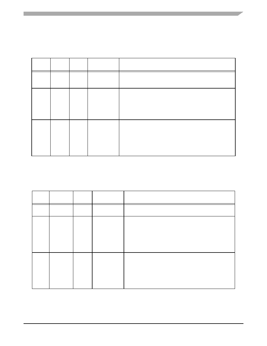
Table 2-5 PLL and Clock
No. of
Pins
Signal
Name
Signal
Type
State During
Reset
Signal Description
1
EXTAL
Input
External Crystal Oscillator Input—This input should be
connected to an 8MHz external crystal or ceramic resonator. For
more information, please refer to Section 3.5.
1
XTAL
Input/O
utput
Chip-driven
Crystal Oscillator Output—This output should be connected to
an 8MHz external crystal or ceramic resonator. For more
information, please refer to Section 3.5.
This pin can also be connected to an external clock source. For
more information, please refer to Section 3.5.3.
1
CLKO
Output
Chip-driven
Clock Output—This pin outputs a buffered clock signal. By
programming the CLKOSEL[4:0] bits in the CLKO Select
Register (CLKOSR), the user can select between outputting a
version of the signal applied to XTAL and a version of the
device’s master clock at the output of the PLL. The clock
frequency on this pin can also be disabled by programming the
CLKOSEL[4:0] bits in CLKOSR.
Table 2-6 Address Bus Signals
No. of
Pins
Signal
Name
Signal
Type
State During
Reset
Signal Description
6
A0–A5
Output
Tri-stated
Address Bus—A0–A5 specify the address for external
Program or Data memory accesses.
2
A6–A7
GPIOE2–
GPIOE3
Output
Input/O
utput
Tri-stated
Input
Address Bus—A6–A7 specify the address for external
Program or Data memory accesses.
Port E GPIO—These two General Purpose I/O (GPIO) pins
can be individually programmed as input or output pins.
After reset, the default state is Address Bus.
8
A8–A15
GPIOA0–
GPIOA7
Output
Input/O
utput
Tri-stated
Input
Address Bus—A8–A15 specify the address for external
Program or Data memory accesses.
Port A GPIO—These eight General Purpose I/O (GPIO) pins
can be individually be programmed as input or output pins.
After reset, the default state is Address Bus.
相关PDF资料 |
PDF描述 |
|---|---|
| DSP56F803BU80 | IC DSP 80MHZ 64KB FLASH 100LQFP |
| MC68332ACFC25 | IC MCU 32BIT 25MHZ 132-PQFP |
| MC68332ACFC20 | IC MCU 32BIT 20MHZ 132-PQFP |
| MCF5307FT66B | IC MPU 32BIT COLDF 66MHZ 208FQFP |
| MCF5206FT25A | IC MCU 32BIT COLDF 25MHZ 160-QFP |
相关代理商/技术参数 |
参数描述 |
|---|---|
| DSP56F805FV80E | 功能描述:数字信号处理器和控制器 - DSP, DSC 80Mhz/40MIPS RoHS:否 制造商:Microchip Technology 核心:dsPIC 数据总线宽度:16 bit 程序存储器大小:16 KB 数据 RAM 大小:2 KB 最大时钟频率:40 MHz 可编程输入/输出端数量:35 定时器数量:3 设备每秒兆指令数:50 MIPs 工作电源电压:3.3 V 最大工作温度:+ 85 C 封装 / 箱体:TQFP-44 安装风格:SMD/SMT |
| DSP56F805FV80E | 制造商:Freescale Semiconductor 功能描述:Digital Signal Processor IC DSP Type:Cor |
| DSP56F805FV80E | 制造商:Freescale Semiconductor 功能描述:DSP LQFP144 3.6V |
| DSP56F805PB | 制造商:未知厂家 制造商全称:未知厂家 功能描述:56F805 16-Bit Hybrid Controller Product Brief |
| DSP56F807 | 制造商:MOTOROLA 制造商全称:Motorola, Inc 功能描述:56F807 16-bit Hybrid Processor |
发布紧急采购,3分钟左右您将得到回复。