- 您现在的位置:买卖IC网 > PDF目录3851 > DSPIC30F2010-20I/SP (Microchip Technology)IC DSPIC MCU/DSP 12K 28DIP PDF资料下载
参数资料
| 型号: | DSPIC30F2010-20I/SP |
| 厂商: | Microchip Technology |
| 文件页数: | 47/66页 |
| 文件大小: | 0K |
| 描述: | IC DSPIC MCU/DSP 12K 28DIP |
| 产品培训模块: | Asynchronous Stimulus |
| 标准包装: | 15 |
| 系列: | dsPIC™ 30F |
| 核心处理器: | dsPIC |
| 芯体尺寸: | 16-位 |
| 速度: | 20 MIPS |
| 连通性: | I²C,SPI,UART/USART |
| 外围设备: | 高级欠压探测/复位,电机控制 PWM,QEI,POR,PWM,WDT |
| 输入/输出数: | 20 |
| 程序存储器容量: | 12KB(4K x 24) |
| 程序存储器类型: | 闪存 |
| EEPROM 大小: | 1K x 8 |
| RAM 容量: | 512 x 8 |
| 电压 - 电源 (Vcc/Vdd): | 2.5 V ~ 5.5 V |
| 数据转换器: | A/D 6x10b |
| 振荡器型: | 内部 |
| 工作温度: | -40°C ~ 85°C |
| 封装/外壳: | 28-DIP(0.300",7.62mm) |
| 包装: | 管件 |
| 产品目录页面: | 650 (CN2011-ZH PDF) |
| 配用: | DV164005-ND - KIT ICD2 SIMPLE SUIT W/USB CABLE |
| 其它名称: | DSPIC30F2010-20I/SPG DSPIC30F201020ISG DSPIC30F201020ISG-ND DSPIC30F201020ISP |
第1页第2页第3页第4页第5页第6页第7页第8页第9页第10页第11页第12页第13页第14页第15页第16页第17页第18页第19页第20页第21页第22页第23页第24页第25页第26页第27页第28页第29页第30页第31页第32页第33页第34页第35页第36页第37页第38页第39页第40页第41页第42页第43页第44页第45页第46页当前第47页第48页第49页第50页第51页第52页第53页第54页第55页第56页第57页第58页第59页第60页第61页第62页第63页第64页第65页第66页
2010 Microchip Technology Inc.
DS70102K-page 51
dsPIC30F Flash Programming Specification
11.11 Reading Configuration Memory
The procedure for reading configuration memory is
similar to the procedure for reading code memory,
except that 16-bit data words are read instead of 24-bit
words. Since there are seven Configuration registers,
they are read one register at a time.
Table 11-11 shows the ICSP programming details for
reading all of the configuration memory. Note that the
TBLPAG register is hard-coded to 0xF8 (the upper byte
address of configuration memory), and the read pointer
W6 is initialized to 0x0000.
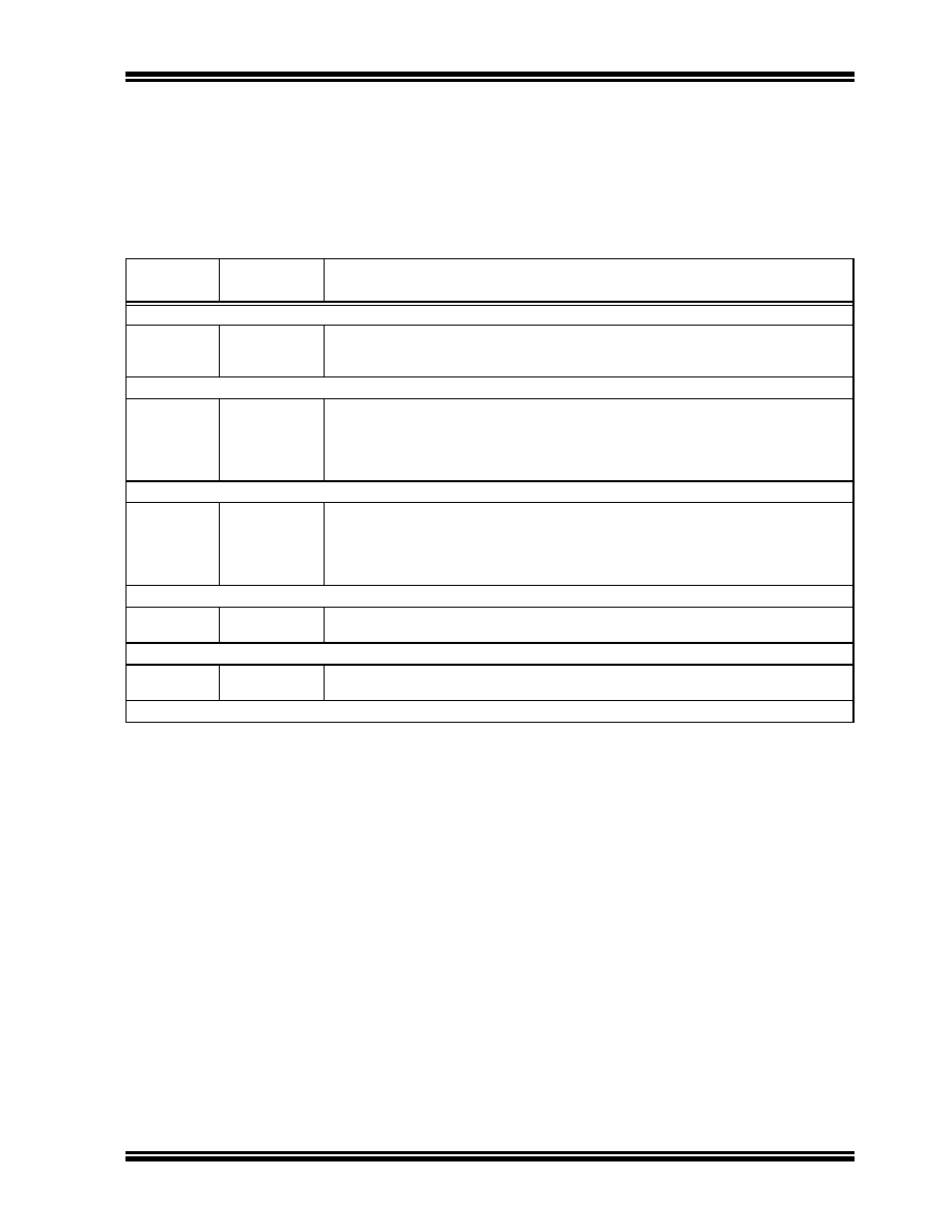
TABLE 11-11: SERIAL INSTRUCTION EXECUTION FOR READING ALL CONFIGURATION MEMORY
Command
(Binary)
Data
(Hexadecimal)
Description
Step 1: Exit the Reset vector.
0000
040100
000000
GOTO 0x100
NOP
Step 2: Initialize TBLPAG, and the read pointer (W6) and the write pointer (W7) for TBLRD instruction.
0000
200F80
880190
EB0300
EB0380
000000
MOV
#0xF8, W0
MOV
W0, TBLPAG
CLR
W6
CLR
W7
NOP
Step 3: Read the Configuration register and write it to the VISI register (located at 0x784).
0000
BA0BB6
000000
883C20
000000
TBLRDL [W6++], [W7]
NOP
MOV
W0, VISI
NOP
Step 4: Output the VISI register using the REGOUT command.
0001
0000
<VISI>
000000
Clock out contents of VISI register
NOP
Step 5: Reset device internal PC.
0000
040100
000000
GOTO 0x100
NOP
Step 6: Repeat steps 3-5 six times to read all of configuration memory.
相关PDF资料 |
PDF描述 |
|---|---|
| AT89S52-24AC | IC MCU 8K FLASH 24MHZ 44-TQFP |
| AT89S51-24PI | IC 8051 MCU 4K FLASH 40-DIP |
| AT89S51-24PC | IC 8051 MCU 4K FLASH 40-DIP |
| AT89LV55-12PC | IC 8051 MCU FLASH 20K 40DIP |
| AT89LV55-12JI | IC 8051 MCU FLASH 20K 44PLCC |
相关代理商/技术参数 |
参数描述 |
|---|---|
| DSPIC30F2010-30I | 制造商:MICROCHIP 制造商全称:Microchip Technology 功能描述:High-Performance, 16-bit Digital Signal Controllers |
| dsPIC30F2010-30I/MM | 功能描述:数字信号处理器和控制器 - DSP, DSC 16B MCU DSP 28LD 20MIPS 12KB FLASH RoHS:否 制造商:Microchip Technology 核心:dsPIC 数据总线宽度:16 bit 程序存储器大小:16 KB 数据 RAM 大小:2 KB 最大时钟频率:40 MHz 可编程输入/输出端数量:35 定时器数量:3 设备每秒兆指令数:50 MIPs 工作电源电压:3.3 V 最大工作温度:+ 85 C 封装 / 箱体:TQFP-44 安装风格:SMD/SMT |
| DSPIC30F2010-30I/MMG | 功能描述:数字信号处理器和控制器 - DSP, DSC 16bit Signal Cntrlr Lead Free Package RoHS:否 制造商:Microchip Technology 核心:dsPIC 数据总线宽度:16 bit 程序存储器大小:16 KB 数据 RAM 大小:2 KB 最大时钟频率:40 MHz 可编程输入/输出端数量:35 定时器数量:3 设备每秒兆指令数:50 MIPs 工作电源电压:3.3 V 最大工作温度:+ 85 C 封装 / 箱体:TQFP-44 安装风格:SMD/SMT |
| DSPIC30F2010-30I/SO | 功能描述:数字信号处理器和控制器 - DSP, DSC 20MHz 12KB Flash RoHS:否 制造商:Microchip Technology 核心:dsPIC 数据总线宽度:16 bit 程序存储器大小:16 KB 数据 RAM 大小:2 KB 最大时钟频率:40 MHz 可编程输入/输出端数量:35 定时器数量:3 设备每秒兆指令数:50 MIPs 工作电源电压:3.3 V 最大工作温度:+ 85 C 封装 / 箱体:TQFP-44 安装风格:SMD/SMT |
| DSPIC30F2010-30I/SOG | 功能描述:数字信号处理器和控制器 - DSP, DSC 16bit Signal Cntrlr RoHS:否 制造商:Microchip Technology 核心:dsPIC 数据总线宽度:16 bit 程序存储器大小:16 KB 数据 RAM 大小:2 KB 最大时钟频率:40 MHz 可编程输入/输出端数量:35 定时器数量:3 设备每秒兆指令数:50 MIPs 工作电源电压:3.3 V 最大工作温度:+ 85 C 封装 / 箱体:TQFP-44 安装风格:SMD/SMT |
发布紧急采购,3分钟左右您将得到回复。