- 您现在的位置:买卖IC网 > PDF目录21337 > DSPIC33FJ12MC201T-I/SS (Microchip Technology)IC DSPIC MCU/DSP 12K 20SSOP PDF资料下载
参数资料
| 型号: | DSPIC33FJ12MC201T-I/SS |
| 厂商: | Microchip Technology |
| 文件页数: | 143/155页 |
| 文件大小: | 0K |
| 描述: | IC DSPIC MCU/DSP 12K 20SSOP |
| 产品培训模块: | Asynchronous Stimulus |
| 标准包装: | 1,600 |
| 系列: | dsPIC™ 33F |
| 核心处理器: | dsPIC |
| 芯体尺寸: | 16-位 |
| 速度: | 40 MIP |
| 连通性: | I²C,IrDA,SPI,UART/USART |
| 外围设备: | 高级欠压探测/复位,电机控制 PWM,QEI,POR,PWM,WDT |
| 输入/输出数: | 15 |
| 程序存储器容量: | 12KB(12K x 8) |
| 程序存储器类型: | 闪存 |
| RAM 容量: | 1K x 8 |
| 电压 - 电源 (Vcc/Vdd): | 3 V ~ 3.6 V |
| 数据转换器: | A/D 4x10b |
| 振荡器型: | 内部 |
| 工作温度: | -40°C ~ 85°C |
| 封装/外壳: | 20-SSOP(0.209",5.30mm 宽) |
| 包装: | 带卷 (TR) |
| 配用: | DV164033-ND - KIT START EXPLORER 16 MPLAB ICD2 DM240001-ND - BOARD DEMO PIC24/DSPIC33/PIC32 |
| 其它名称: | DSPIC33FJ12MC201T-I/SSTR |
第1页第2页第3页第4页第5页第6页第7页第8页第9页第10页第11页第12页第13页第14页第15页第16页第17页第18页第19页第20页第21页第22页第23页第24页第25页第26页第27页第28页第29页第30页第31页第32页第33页第34页第35页第36页第37页第38页第39页第40页第41页第42页第43页第44页第45页第46页第47页第48页第49页第50页第51页第52页第53页第54页第55页第56页第57页第58页第59页第60页第61页第62页第63页第64页第65页第66页第67页第68页第69页第70页第71页第72页第73页第74页第75页第76页第77页第78页第79页第80页第81页第82页第83页第84页第85页第86页第87页第88页第89页第90页第91页第92页第93页第94页第95页第96页第97页第98页第99页第100页第101页第102页第103页第104页第105页第106页第107页第108页第109页第110页第111页第112页第113页第114页第115页第116页第117页第118页第119页第120页第121页第122页第123页第124页第125页第126页第127页第128页第129页第130页第131页第132页第133页第134页第135页第136页第137页第138页第139页第140页第141页第142页当前第143页第144页第145页第146页第147页第148页第149页第150页第151页第152页第153页第154页第155页
88
A/T89C51AC2
4127H–8051–02/08
ADC Converter
Operation
A start of single A/D conversion is triggered by setting bit ADSST (ADCON.3).
After completion of the A/D conversion, the ADSST bit is cleared by hardware.
The end-of-conversion flag ADEOC (ADCON.4) is set when the value of conversion is
available in ADDH and ADDL, it must be cleared by software. If the bit EADC (IEN1.1) is
set, an interrupt occur when flag ADEOC is set (see Figure 48). Clear this flag for re-
arming the interrupt.
The bits SCH0 to SCH2 in ADCON register are used for the analog input channel
selection.(1)
Note:
1. Always leave Tsetup time before starting a conversion unless ADEN is permanently
high. In this case one should wait Tsetup only before the first conversion.
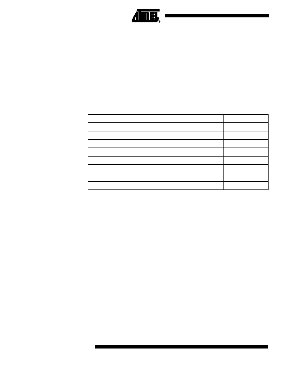
Table 62. Selected Analog input
Voltage Conversion
When the ADCIN is equals to VAREF the ADC converts the signal to 3FFh (full scale). If
the input voltage equals VAGND, the ADC converts it to 000h. Input voltage between
VAREF and VAGND are a straight-line linear conversion. All other voltages will result in
3FFh if greater than VAREF and 000h if less than VAGND.
Note:
ADCIN should not exceed VAREF absolute maximum range (see “Absolute Maximum
Clock Selection
The ADC clock is the same as CPU.
The maximum clock frequency is defined in the DC parmeter for A/D converter. A pres-
caler is featured (ADCCLK) to generate the ADC clock from the oscillator frequency.
if PRS > 0 then fADC = Fperiph / 2 x PRS
if PRS = 0 then fADC = Fperiph / 64
SCH2
SCH1
SCH0
Selected Analog input
0
AN0
0
1
AN1
0
1
0
AN2
0
1
AN3
1
0
AN4
1
0
1
AN5
1
0
AN6
1
AN7
相关PDF资料 |
PDF描述 |
|---|---|
| CR7310-LL-120-.11-A-CD-ELR-I | GRND FAULT SENS LATCH 120V |
| P51-500-S-G-P-20MA-000-000 | SENSOR 500PSIS 1/8 NPT 4-20 MA |
| P51-15-A-S-D-4.5OVP-000-000 | SENSOR 15PSI 1/4-18NPT .5-4.5V |
| REC5-1215SRW/H4/A/M/CTRL | CONV DC/DC 5W 9-18VIN 15VOUT |
| P51-200-G-W-MD-5V-000-000 | SENSOR 200PSI 1/8-27NPT 1-5V |
相关代理商/技术参数 |
参数描述 |
|---|---|
| dsPIC33FJ12MC202-E/ML | 功能描述:数字信号处理器和控制器 - DSP, DSC 12KB FLSH 1024BRAM 16B nanoWatt RoHS:否 制造商:Microchip Technology 核心:dsPIC 数据总线宽度:16 bit 程序存储器大小:16 KB 数据 RAM 大小:2 KB 最大时钟频率:40 MHz 可编程输入/输出端数量:35 定时器数量:3 设备每秒兆指令数:50 MIPs 工作电源电压:3.3 V 最大工作温度:+ 85 C 封装 / 箱体:TQFP-44 安装风格:SMD/SMT |
| dsPIC33FJ12MC202-E/SO | 功能描述:数字信号处理器和控制器 - DSP, DSC 12KB FLSH 1024BRAM 16B nanoWatt RoHS:否 制造商:Microchip Technology 核心:dsPIC 数据总线宽度:16 bit 程序存储器大小:16 KB 数据 RAM 大小:2 KB 最大时钟频率:40 MHz 可编程输入/输出端数量:35 定时器数量:3 设备每秒兆指令数:50 MIPs 工作电源电压:3.3 V 最大工作温度:+ 85 C 封装 / 箱体:TQFP-44 安装风格:SMD/SMT |
| dsPIC33FJ12MC202-E/SP | 功能描述:数字信号处理器和控制器 - DSP, DSC 12KB FLSH 1024BRAM 16B nanoWatt RoHS:否 制造商:Microchip Technology 核心:dsPIC 数据总线宽度:16 bit 程序存储器大小:16 KB 数据 RAM 大小:2 KB 最大时钟频率:40 MHz 可编程输入/输出端数量:35 定时器数量:3 设备每秒兆指令数:50 MIPs 工作电源电压:3.3 V 最大工作温度:+ 85 C 封装 / 箱体:TQFP-44 安装风格:SMD/SMT |
| dsPIC33FJ12MC202-E/SS | 功能描述:数字信号处理器和控制器 - DSP, DSC 16B Microcontrollers RoHS:否 制造商:Microchip Technology 核心:dsPIC 数据总线宽度:16 bit 程序存储器大小:16 KB 数据 RAM 大小:2 KB 最大时钟频率:40 MHz 可编程输入/输出端数量:35 定时器数量:3 设备每秒兆指令数:50 MIPs 工作电源电压:3.3 V 最大工作温度:+ 85 C 封装 / 箱体:TQFP-44 安装风格:SMD/SMT |
| dsPIC33FJ12MC202-I/ML | 功能描述:数字信号处理器和控制器 - DSP, DSC 212KB Flash 1024BRAM 40MIPS RoHS:否 制造商:Microchip Technology 核心:dsPIC 数据总线宽度:16 bit 程序存储器大小:16 KB 数据 RAM 大小:2 KB 最大时钟频率:40 MHz 可编程输入/输出端数量:35 定时器数量:3 设备每秒兆指令数:50 MIPs 工作电源电压:3.3 V 最大工作温度:+ 85 C 封装 / 箱体:TQFP-44 安装风格:SMD/SMT |
发布紧急采购,3分钟左右您将得到回复。