- 您现在的位置:买卖IC网 > PDF目录21337 > DSPIC33FJ12MC201T-I/SS (Microchip Technology)IC DSPIC MCU/DSP 12K 20SSOP PDF资料下载
参数资料
| 型号: | DSPIC33FJ12MC201T-I/SS |
| 厂商: | Microchip Technology |
| 文件页数: | 55/155页 |
| 文件大小: | 0K |
| 描述: | IC DSPIC MCU/DSP 12K 20SSOP |
| 产品培训模块: | Asynchronous Stimulus |
| 标准包装: | 1,600 |
| 系列: | dsPIC™ 33F |
| 核心处理器: | dsPIC |
| 芯体尺寸: | 16-位 |
| 速度: | 40 MIP |
| 连通性: | I²C,IrDA,SPI,UART/USART |
| 外围设备: | 高级欠压探测/复位,电机控制 PWM,QEI,POR,PWM,WDT |
| 输入/输出数: | 15 |
| 程序存储器容量: | 12KB(12K x 8) |
| 程序存储器类型: | 闪存 |
| RAM 容量: | 1K x 8 |
| 电压 - 电源 (Vcc/Vdd): | 3 V ~ 3.6 V |
| 数据转换器: | A/D 4x10b |
| 振荡器型: | 内部 |
| 工作温度: | -40°C ~ 85°C |
| 封装/外壳: | 20-SSOP(0.209",5.30mm 宽) |
| 包装: | 带卷 (TR) |
| 配用: | DV164033-ND - KIT START EXPLORER 16 MPLAB ICD2 DM240001-ND - BOARD DEMO PIC24/DSPIC33/PIC32 |
| 其它名称: | DSPIC33FJ12MC201T-I/SSTR |
第1页第2页第3页第4页第5页第6页第7页第8页第9页第10页第11页第12页第13页第14页第15页第16页第17页第18页第19页第20页第21页第22页第23页第24页第25页第26页第27页第28页第29页第30页第31页第32页第33页第34页第35页第36页第37页第38页第39页第40页第41页第42页第43页第44页第45页第46页第47页第48页第49页第50页第51页第52页第53页第54页当前第55页第56页第57页第58页第59页第60页第61页第62页第63页第64页第65页第66页第67页第68页第69页第70页第71页第72页第73页第74页第75页第76页第77页第78页第79页第80页第81页第82页第83页第84页第85页第86页第87页第88页第89页第90页第91页第92页第93页第94页第95页第96页第97页第98页第99页第100页第101页第102页第103页第104页第105页第106页第107页第108页第109页第110页第111页第112页第113页第114页第115页第116页第117页第118页第119页第120页第121页第122页第123页第124页第125页第126页第127页第128页第129页第130页第131页第132页第133页第134页第135页第136页第137页第138页第139页第140页第141页第142页第143页第144页第145页第146页第147页第148页第149页第150页第151页第152页第153页第154页第155页
PIC18F2XK20/4XK20
DS41303G-page 282
2010 Microchip Technology Inc.
20.4
Comparator Interrupt Operation
The comparator interrupt flag can be set whenever
there is a change in the output value of the comparator.
Changes are recognized by means of a mismatch
circuit which consists of two latches and an exclusive-
or gate (see Figure 20-2 and Figure 20-3). One latch is
updated with the comparator output level when the
CMxCON0 register is read. This latch retains the value
until the next read of the CMxCON0 register or the
occurrence of a Reset. The other latch of the mismatch
circuit is updated on every Q1 system clock. A
mismatch condition will occur when a comparator
output change is clocked through the second latch on
the Q1 clock cycle. At this point the two mismatch
latches have opposite output levels which is detected
by the exclusive-or gate and fed to the interrupt
circuitry. The mismatch condition persists until either
the CMxCON0 register is read or the comparator
output returns to the previous state.
The comparator interrupt is set by the mismatch edge
and not the mismatch level. This means that the inter-
rupt flag can be reset without the additional step of
reading or writing the CMxCON0 register to clear the
mismatch registers. When the mismatch registers are
cleared, an interrupt will occur upon the comparator’s
return to the previous state, otherwise no interrupt will
be generated.
Software will need to maintain information about the
status of the comparator output, as read from the
CMxCON0 register, or CM2CON1 register, to determine
the actual change that has occurred. See Figures 20-4
and 20-5.
The CxIF bit of the PIR2 register is the comparator
interrupt flag. This bit must be reset by software by
clearing it to ‘0’. Since it is also possible to write a ‘1’ to
this register, an interrupt can be generated.
In mid-range Compatibility mode the CxIE bit of the
PIE2 register and the PEIE and GIE bits of the INTCON
register must all be set to enable comparator interrupts.
If any of these bits are cleared, the interrupt is not
enabled, although the CxIF bit of the PIR2 register will
still be set if an interrupt condition occurs.
20.4.1
PRESETTING THE MISMATCH
LATCHES
The comparator mismatch latches can be preset to the
desired state before the comparators are enabled.
When the comparator is off the CxPOL bit controls the
CxOUT level. Set the CxPOL bit to the desired CxOUT
non-interrupt level while the CxON bit is cleared. Then,
configure the desired CxPOL level in the same instruc-
tion that the CxON bit is set. Since all register writes are
performed as a Read-Modify-Write, the mismatch
latches will be cleared during the instruction Read
phase and the actual configuration of the CxON and
CxPOL bits will be occur in the final Write phase.
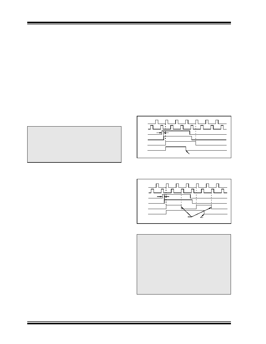
FIGURE 20-4:
COMPARATOR
INTERRUPT TIMING W/O
CMxCON0 READ
FIGURE 20-5:
COMPARATOR
INTERRUPT TIMING WITH
CMxCON0 READ
Note 1: A write operation to the CMxCON0
register will also clear the mismatch
condition because all writes include a read
operation at the beginning of the write
cycle.
2: Comparator interrupts will operate correctly
regardless of the state of CxOE.
Note 1: If a change in the CMxCON0 register
(CxOUT) should occur when a read oper-
ation is being executed (start of the Q2
cycle), then the CxIF interrupt flag of the
PIR2 register may not get set.
2: When either comparator is first enabled,
bias circuitry in the Comparator module
may cause an invalid output from the
comparator until the bias circuitry is stable.
Allow about 1
s for bias settling then clear
the mismatch condition and interrupt flags
before enabling comparator interrupts.
Q1
Q3
CxIN+
CxOUT
Set CxIF (edge)
CxIF
TRT
reset by software
Q1
Q3
CxIN+
CxOUT
Set CxIF (edge)
CxIF
TRT
reset by software
cleared by CMxCON0 read
相关PDF资料 |
PDF描述 |
|---|---|
| CR7310-LL-120-.11-A-CD-ELR-I | GRND FAULT SENS LATCH 120V |
| P51-500-S-G-P-20MA-000-000 | SENSOR 500PSIS 1/8 NPT 4-20 MA |
| P51-15-A-S-D-4.5OVP-000-000 | SENSOR 15PSI 1/4-18NPT .5-4.5V |
| REC5-1215SRW/H4/A/M/CTRL | CONV DC/DC 5W 9-18VIN 15VOUT |
| P51-200-G-W-MD-5V-000-000 | SENSOR 200PSI 1/8-27NPT 1-5V |
相关代理商/技术参数 |
参数描述 |
|---|---|
| dsPIC33FJ12MC202-E/ML | 功能描述:数字信号处理器和控制器 - DSP, DSC 12KB FLSH 1024BRAM 16B nanoWatt RoHS:否 制造商:Microchip Technology 核心:dsPIC 数据总线宽度:16 bit 程序存储器大小:16 KB 数据 RAM 大小:2 KB 最大时钟频率:40 MHz 可编程输入/输出端数量:35 定时器数量:3 设备每秒兆指令数:50 MIPs 工作电源电压:3.3 V 最大工作温度:+ 85 C 封装 / 箱体:TQFP-44 安装风格:SMD/SMT |
| dsPIC33FJ12MC202-E/SO | 功能描述:数字信号处理器和控制器 - DSP, DSC 12KB FLSH 1024BRAM 16B nanoWatt RoHS:否 制造商:Microchip Technology 核心:dsPIC 数据总线宽度:16 bit 程序存储器大小:16 KB 数据 RAM 大小:2 KB 最大时钟频率:40 MHz 可编程输入/输出端数量:35 定时器数量:3 设备每秒兆指令数:50 MIPs 工作电源电压:3.3 V 最大工作温度:+ 85 C 封装 / 箱体:TQFP-44 安装风格:SMD/SMT |
| dsPIC33FJ12MC202-E/SP | 功能描述:数字信号处理器和控制器 - DSP, DSC 12KB FLSH 1024BRAM 16B nanoWatt RoHS:否 制造商:Microchip Technology 核心:dsPIC 数据总线宽度:16 bit 程序存储器大小:16 KB 数据 RAM 大小:2 KB 最大时钟频率:40 MHz 可编程输入/输出端数量:35 定时器数量:3 设备每秒兆指令数:50 MIPs 工作电源电压:3.3 V 最大工作温度:+ 85 C 封装 / 箱体:TQFP-44 安装风格:SMD/SMT |
| dsPIC33FJ12MC202-E/SS | 功能描述:数字信号处理器和控制器 - DSP, DSC 16B Microcontrollers RoHS:否 制造商:Microchip Technology 核心:dsPIC 数据总线宽度:16 bit 程序存储器大小:16 KB 数据 RAM 大小:2 KB 最大时钟频率:40 MHz 可编程输入/输出端数量:35 定时器数量:3 设备每秒兆指令数:50 MIPs 工作电源电压:3.3 V 最大工作温度:+ 85 C 封装 / 箱体:TQFP-44 安装风格:SMD/SMT |
| dsPIC33FJ12MC202-I/ML | 功能描述:数字信号处理器和控制器 - DSP, DSC 212KB Flash 1024BRAM 40MIPS RoHS:否 制造商:Microchip Technology 核心:dsPIC 数据总线宽度:16 bit 程序存储器大小:16 KB 数据 RAM 大小:2 KB 最大时钟频率:40 MHz 可编程输入/输出端数量:35 定时器数量:3 设备每秒兆指令数:50 MIPs 工作电源电压:3.3 V 最大工作温度:+ 85 C 封装 / 箱体:TQFP-44 安装风格:SMD/SMT |
发布紧急采购,3分钟左右您将得到回复。