- 您现在的位置:买卖IC网 > PDF目录97873 > E6420-EDGE6420 Per-Pin Electronics Companion DAC PDF资料下载
参数资料
| 型号: | E6420-EDGE6420 |
| 英文描述: | Per-Pin Electronics Companion DAC |
| 中文描述: | 按针脚电子伴侣援 |
| 文件页数: | 4/29页 |
| 文件大小: | 244K |
| 代理商: | E6420-EDGE6420 |
第1页第2页第3页当前第4页第5页第6页第7页第8页第9页第10页第11页第12页第13页第14页第15页第16页第17页第18页第19页第20页第21页第22页第23页第24页第25页第26页第27页第28页第29页
12
2000 Semtech Corp.
www .semtech.com
HIGH-PERFORMANCE PRODUCTS – ATE
Edge6420
Circuit Description (continued)
Programming Sequence
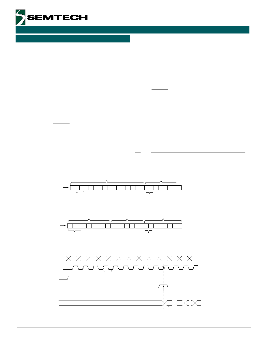
The DACs are programmed serially (see Figures 1, 2a,
2b, and 3). On each rising edge of CK, SDI is loaded into
a shift register. It requires 24 Clocks to fully load the shift
register (8 address bits + 16 data bits).
For Groups A, B, C, D, and E DACs:
Address and data are loaded LSB first, MSB last. In a 24
clock sequence, A0, as shown in Figure 2a, is loaded into
the shift register on the first CK rising edge, and D15 is
loaded last on the 24th rising CK edge. Note that a 24th
falling CK edge is required to transfer the data from the
Central DAC Latch to the selected DAC latch (See Figure
1).
See detailed Timing Diagrams in the "AC
Characteristics" specifications section.
For Group F DACs:
The loading sequence is the same as Groups A-E, but
Group F uses only 6 bits, and these bits must be
programmed as shown in Figure 2b. 24 clock cycles are
required for programming, with A0 loaded on the first rising
CK edge, and D8 (as shown in Figure 2b) loaded on the
24th rising CK edge.
As is the case with other groups, a 24th falling edge of
CK24 is required for proper programming of Group F DACs.
Chip Enable
CE is a synchronous input which determines whether the
Central DAC latch shown in Figure 1 is loaded with data
from the shift register. CE is also necessary to update a
DAC. If CE is high, rising edges of CK load data from the
shift register to an internal latch. If CE is low, central DAC
latch updating is disabled.
CE
Central and Individual DAC Latch "Load" Status
low
Central and individual DAC latch loading is
disabled
high
Central and individual DAC latches are loaded
Figure 2a. Format of Address and Data in Shift Register for Group A, B, C, D, and E DACs (13-bits)
Figure 2b. Format of Address and Data in Shift Register for Group F DACs (6-bits)
Figure 3. Serial Data Programming Sequence
D15 D14 D13 D12 D11
D10
D9
D8
D7
D6
D5
D4
D3
D2
D1
D0
DATA
A5
A4
A3
A2
A1
A0
ADDRESS
LSB
Bits reserved for
future upgradability
SDI
A6
Bits reserved for
future upgradability
LSB
MSB
A7
D5
D8
D7
D6
D4
D3
D2
D1
D0
X
A6
A5
A4
A3
A2
A1
A0
LSB
Bits reserved for
future upgradability
SDI
A7
Bits reserved for
future upgradability
"Don't Care" bits that must be
included in programming sequence
LSB
MSB
DATA
ADDRESS
A0
A1
A6
A7
D0
D1
D14
D15
LSB
Addr.
MSB
Addr.
LSB
Data
MSB
Data
SDI
CK
≈
A1
CE
UPDATE
Next Set
of Data
A0
CK1
≈
Update Selected
DAC Register
SDO
CK24
A0
A1
Previous Data
≈
Corresponds to
A0 loaded at CK1
TCK
相关PDF资料 |
PDF描述 |
|---|---|
| E646-EDGE646 | Pin Electronics Driver. Window Comparator. and Switch Matrix |
| E647-EDGE647 | Pin Electronics Driver. Window Comparator. and Switch Matrix |
| E649-EDGE649 | Octal Pin Electronics Driver / Receiver |
| E670-EDGE670 | 500 MHz Window Comparator |
| E672-EDGE672 | 500 MHz Pin Electronics Window Comparator and Load |
相关代理商/技术参数 |
参数描述 |
|---|---|
| E642123BIN WAF | 制造商:Texas Instruments 功能描述: |
| E642325A1N WAF | 制造商:Texas Instruments 功能描述: |
| E642332 | 制造商:Elo Touch Solutions Inc 功能描述:1919L, 18.5-INCH LCD, ACCUTOUCH, DUAL SERIAL/USB CONTROLLER, - Bulk |
| E642633 WAF | 制造商:Texas Instruments 功能描述: |
| E642919 WAF | 制造商:Texas Instruments 功能描述: |
发布紧急采购,3分钟左右您将得到回复。