- 您现在的位置:买卖IC网 > PDF目录97873 > E6420-EDGE6420 Per-Pin Electronics Companion DAC PDF资料下载
参数资料
| 型号: | E6420-EDGE6420 |
| 英文描述: | Per-Pin Electronics Companion DAC |
| 中文描述: | 按针脚电子伴侣援 |
| 文件页数: | 9/29页 |
| 文件大小: | 244K |
| 代理商: | E6420-EDGE6420 |
第1页第2页第3页第4页第5页第6页第7页第8页当前第9页第10页第11页第12页第13页第14页第15页第16页第17页第18页第19页第20页第21页第22页第23页第24页第25页第26页第27页第28页第29页
17
2000 Semtech Corp.
www .semtech.com
HIGH-PERFORMANCE PRODUCTS – ATE
Edge6420
Care should be taken to ensure that devices being driven
by Group E and F DACs are designed to be within the
compliance specification.
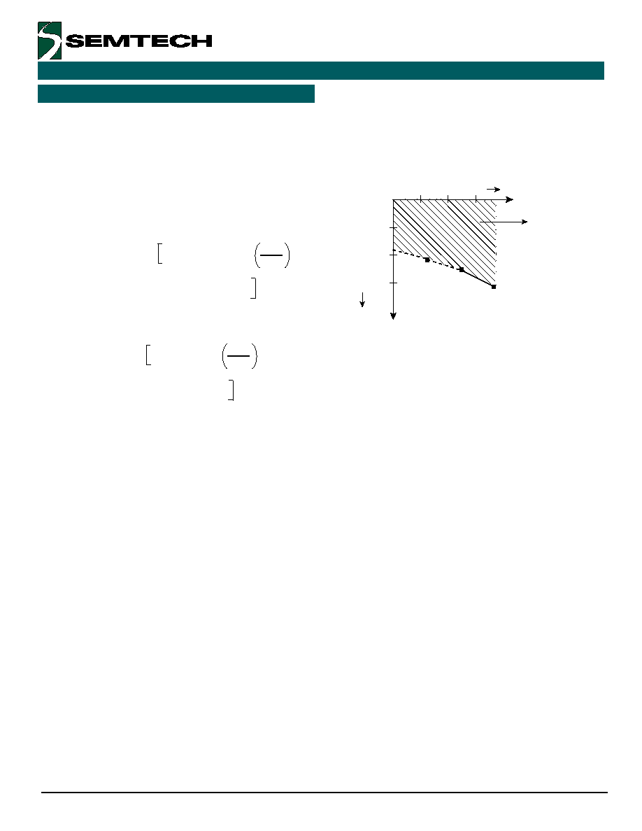
Figure 8. Compliance of Current Output DACs
(Groups E and F)
Caution Regarding Power Dissipation of the 6420
During Parallel Load:
The Voltage DAC output amplifiers, for a FAST process,
can:
Source up to 10 mA (8 mA @ TJ = 100C)
Sink up to 4.5 mA (3.5 mA @ TJ = 100C)
Caution must be taken during a parallel load, particularly
when the voltage DACs are loaded with a large filtering
capacitor (10 to 100 nF). In this scenario, a large voltage
change can induce a large current peak. For example,
the currents calculated below can be induced in the VCC/
VEE supplies:
Source case:
44 DACs * 10 mA / DAC + 40 mA = 480 mA
(or 400 mA @ TJ = 100C) in the VCC supply
Sink case:
44 DACs * 4.5 mA / DAC + 120 mA = 320 mA
(or 280 mA @ TJ = 100C) in the VEE supply
Therefore, the user must take care of extra power
dissipation due to these currents peaks, and should avoid
large voltage changes during a parallel load.
Temperature Coefficient Effect on DACs
There is a gain and offset temperature coefficient that
should be taken into account in the system design that
will affect calibration and performance.
The equation for voltage drift on output DACs is as follows:
VOUT_A,B,C,D = T * TCOFFSET_A,B,C,D
+
CODE * LSB * TCGAIN_A,B,C,D (%/C)
Current outputs drift follow the following equation:
IOUT_E,F = T * TCOFFSET_E,F
+
CODE * LSB * TCGAIN_E,F (%/C)
Average values for TCOFFSET and TCGAIN can be found in
the specifications.
Compliance of Current Output DACs (Groups E, F)
The compliance of the current output DACs (Groups E and
F) is governed by the following two equations:
IOUT < 2.5 mA:
VCOMPLIANCE = (–250 * IOUT) + AVDD – 1.875V
IOUT ≥ 2.5 mA:
VCOMPLIANCE = (–600 * IOUT) + AVDD – 1V
See Figure 8 for a graphical depiction.
Note: IOUT is current sourced from output of DAC.
Application Information (continued)
A
C
V
C
1 mA
2 mA
3 mA
IOUT
AVDD
AVDD – 1
AVDD – 2
AVDD – 3
VCOMPLIANCE
(1.3 mA, AVDD – 2.2V)
(2.5 mA, AVDD – 2.5V)
(3.6 mA, AVDD – 3.2V)
Compliance Exceeded
相关PDF资料 |
PDF描述 |
|---|---|
| E646-EDGE646 | Pin Electronics Driver. Window Comparator. and Switch Matrix |
| E647-EDGE647 | Pin Electronics Driver. Window Comparator. and Switch Matrix |
| E649-EDGE649 | Octal Pin Electronics Driver / Receiver |
| E670-EDGE670 | 500 MHz Window Comparator |
| E672-EDGE672 | 500 MHz Pin Electronics Window Comparator and Load |
相关代理商/技术参数 |
参数描述 |
|---|---|
| E642123BIN WAF | 制造商:Texas Instruments 功能描述: |
| E642325A1N WAF | 制造商:Texas Instruments 功能描述: |
| E642332 | 制造商:Elo Touch Solutions Inc 功能描述:1919L, 18.5-INCH LCD, ACCUTOUCH, DUAL SERIAL/USB CONTROLLER, - Bulk |
| E642633 WAF | 制造商:Texas Instruments 功能描述: |
| E642919 WAF | 制造商:Texas Instruments 功能描述: |
发布紧急采购,3分钟左右您将得到回复。