- 您现在的位置:买卖IC网 > PDF目录97873 > E6420-EDGE6420 Per-Pin Electronics Companion DAC PDF资料下载
参数资料
| 型号: | E6420-EDGE6420 |
| 英文描述: | Per-Pin Electronics Companion DAC |
| 中文描述: | 按针脚电子伴侣援 |
| 文件页数: | 6/29页 |
| 文件大小: | 244K |
| 代理商: | E6420-EDGE6420 |
第1页第2页第3页第4页第5页当前第6页第7页第8页第9页第10页第11页第12页第13页第14页第15页第16页第17页第18页第19页第20页第21页第22页第23页第24页第25页第26页第27页第28页第29页
14
2000 Semtech Corp.
www .semtech.com
HIGH-PERFORMANCE PRODUCTS – ATE
Edge6420
Circuit Description (continued)
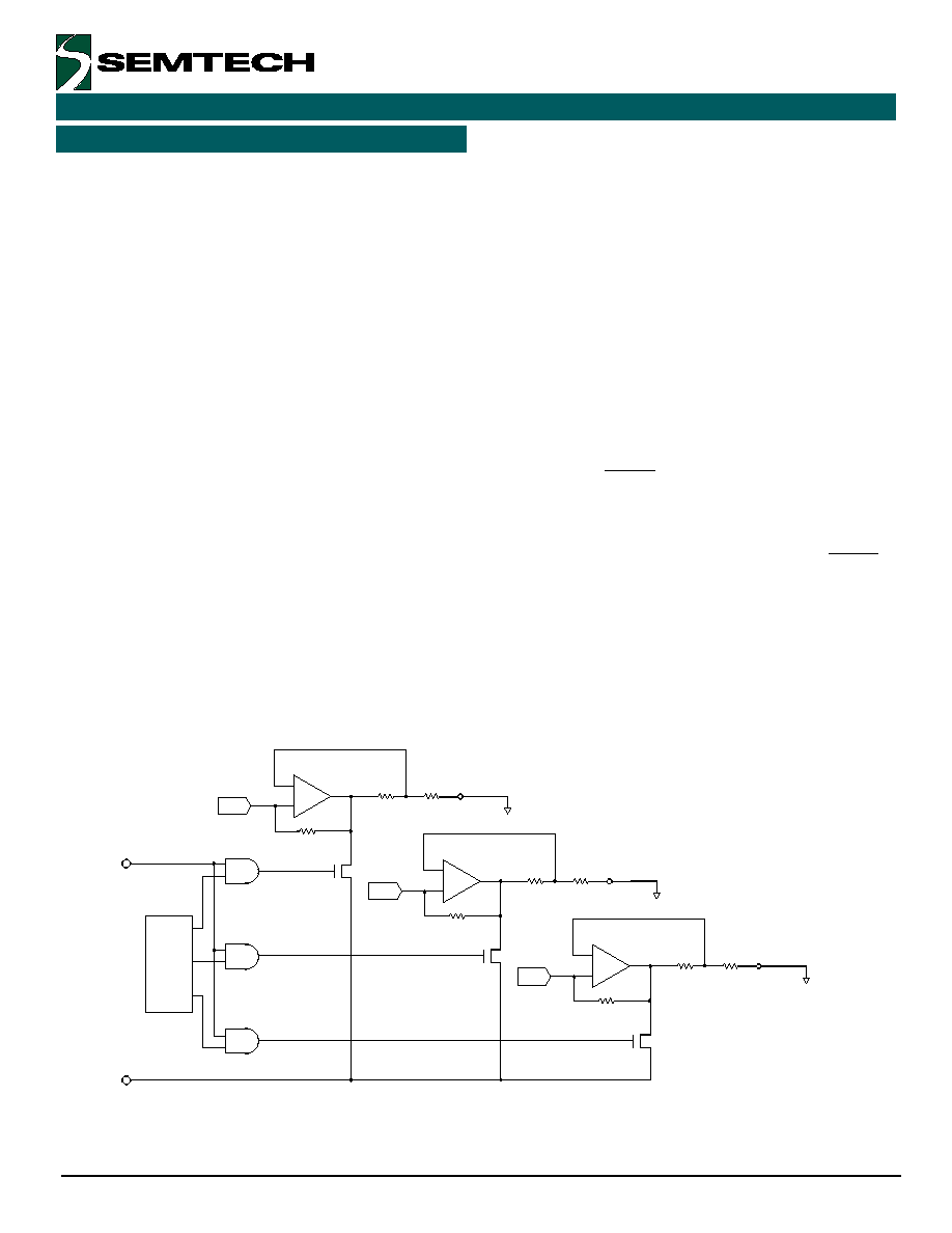
Current Outputs
The TEST_MODE and SCAN_OUT pins on the Edge6420
are used in the same way as for voltage outputs. The
scan circuits for current outputs are shown in Figure 6.
The voltage measured at the SCAN_OUT pin, using the
configuration in Figure 6, for Group E and F current outputs
are as follows:
VSCAN_OUT_E = (RSENSE_E + RPAD) * IOUT_E
where:
RSENSE_E = 400 ± 30%
RPAD = 30 ± 30%
and
VSCAN_OUT_F = (RSENSE_F + RPAD) * IOUT_F
where:
RSENSE_F = 400 ± 30%
RPAD = 30 ± 30%
The typical "ON" resistance of the FET switch is 100 k
,
but can vary from 60 k
to 180 k as a function of process
and output voltage.
Notes when Using SCAN Feature with Multiple Chips
When multiple 6420s are used on a board, and it is desired
to gang the SCAN_OUT pins of these 6420s, or gang the
TEST_MODE inputs to one point, it is required for proper
functioning that the following rules be followed:
1)
If TEST_MODE inputs are ganged together,
SCAN_OUT cannot be ganged, or invalid results
will be observed at the SCAN_OUT pin. Hence,
each SCAN_OUT pin on a 6420 will have to be
measured separately.
2)
If SCAN_OUT is ganged, TEST_MODE pins cannot
be ganged together.
Figure 6. Current Output Scan Circuits
ADDRESS
DECODER
+
–
IOUT_CH0_0
TEST_MODE
SCAN_OUT
IDAC
+
–
IOUT_CH0_1
IDAC
+
–
IOUT_CH0_2
IDAC
CONNECT TO
VIRTUAL GROUND
CONNECT TO
VIRTUAL GROUND
NOTE: WHEN ADDRESS 64 IS INVOKED (PARALLEL LOAD), SCAN IS DISABLED.
CONNECT TO
VIRTUAL GROUND
R
SENSE
R
SENSE
R
PAD
R
PAD
R
PAD
R
SENSE
相关PDF资料 |
PDF描述 |
|---|---|
| E646-EDGE646 | Pin Electronics Driver. Window Comparator. and Switch Matrix |
| E647-EDGE647 | Pin Electronics Driver. Window Comparator. and Switch Matrix |
| E649-EDGE649 | Octal Pin Electronics Driver / Receiver |
| E670-EDGE670 | 500 MHz Window Comparator |
| E672-EDGE672 | 500 MHz Pin Electronics Window Comparator and Load |
相关代理商/技术参数 |
参数描述 |
|---|---|
| E642123BIN WAF | 制造商:Texas Instruments 功能描述: |
| E642325A1N WAF | 制造商:Texas Instruments 功能描述: |
| E642332 | 制造商:Elo Touch Solutions Inc 功能描述:1919L, 18.5-INCH LCD, ACCUTOUCH, DUAL SERIAL/USB CONTROLLER, - Bulk |
| E642633 WAF | 制造商:Texas Instruments 功能描述: |
| E642919 WAF | 制造商:Texas Instruments 功能描述: |
发布紧急采购,3分钟左右您将得到回复。