参数资料
| 型号: | EL5525IREZ-T7 |
| 厂商: | Intersil |
| 文件页数: | 6/10页 |
| 文件大小: | 0K |
| 描述: | IC VREF GEN 18CH TFTLCD 38HTSSOP |
| 标准包装: | 1,000 |
| 应用: | 转换器,TFT,LCD |
| 输入电压: | 4.5 V ~ 16.5 V |
| 输出数: | 18 |
| 输出电压: | 0.5 V ~ 14.95 V |
| 工作温度: | -40°C ~ 85°C |
| 安装类型: | 表面贴装 |
| 封装/外壳: | 38-TFSOP (0.173",4.40mm 宽)裸露焊盘 |
| 供应商设备封装: | 38-TSSOP 裸露焊盘 |
| 包装: | 带卷 (TR) |
�� �
�
�EL5525�
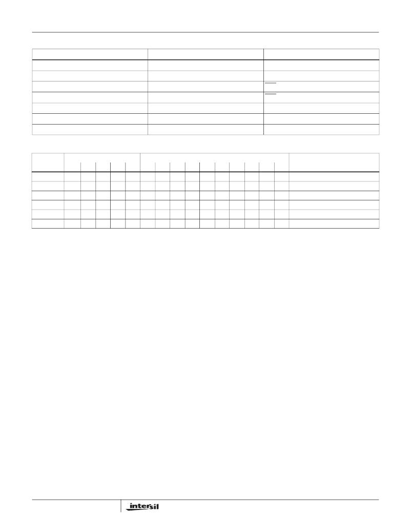
�TABLE� 2.� SERIAL� TIMING� PARAMETERS�
�PARAMETER�
�T�
�t� r� /t� f�
�t� HE�
�t� SE�
�t� HD�
�t� SD�
�t� W�
�RECOMMENDED� OPERATING� RANGE�
�≥� 200ns�
�0.05� *� T�
�≥� 10ns�
�≥� 10ns�
�≥� 10ns�
�≥� 10ns�
�0.50� *� T�
�DESCRIPTION�
�Clock� Period�
�Clock� Rise/Fall� Time�
�ENA� Hold� Time�
�ENA� Setup� Time�
�Data� Hold� Time�
�Data� Setup� Time�
�Clock� Pulse� Width�
�TABLE� 3.� SERIAL� PROGRAMMING� EXAMPLES�
�Control�
�Channel� Address�
�Data�
�C1�
�0�
�0�
�0�
�0�
�0�
�0�
�A4�
�0�
�0�
�0�
�0�
�0�
�1�
�A3�
�0�
�0�
�0�
�0�
�0�
�0�
�A2�
�0�
�0�
�0�
�0�
�1�
�0�
�A1�
�0�
�0�
�0�
�1�
�1�
�0�
�A0�
�0�
�0�
�0�
�1�
�1�
�1�
�D9�
�0�
�1�
�1�
�1�
�0�
�0�
�D8�
�0�
�1�
�0�
�0�
�0�
�0�
�D7�
�0�
�1�
�0�
�0�
�0�
�0�
�D6�
�0�
�1�
�0�
�0�
�0�
�0�
�D5�
�0�
�1�
�0�
�0�
�0�
�0�
�D4�
�0�
�1�
�0�
�0�
�1�
�1�
�D3�
�0�
�1�
�0�
�0�
�1�
�1�
�D2�
�0�
�1�
�0�
�0�
�1�
�1�
�D1�
�0�
�1�
�0�
�0�
�1�
�1�
�D0�
�0�
�1�
�0�
�1�
�1�
�1�
�Condition�
�Channel� A,� Value� =� 0�
�Channel� A,� Value� =� 1023�
�Channel� A,� Value� =� 512�
�Channel� C,� Value� =� 513�
�Channel� H,� Value� =� 31�
�Channel� R,� Value� =� 31�
�Analog� Section�
�Transfer� Function�
�The� transfer� function� is:� shown� in� Equaion� 1:�
�For� transient� load� application,� the� external� clock� Mode�
�should� be� used� to� ensure� all� functions� are� synchronized�
�together.� The� positive� edge� of� the� external� clock� to� the� OSC�
�pin� should� be� timed� to� avoid� the� transient� load� effect.� The�
�V� OUT� (� IDEAL� )� =� V� REFL� +� -------------� � (� V� REFH� -� V� REFL� )�
�data�
�1024�
�(EQ.� 1)�
�Application� Drawing� shows� the� LCD� H� rate� signal� used,� here�
�the� positive� clock� edge� is� timed� to� avoid� the� transient� load� of�
�where� data� is� the� decimal� value� of� the� 10-bit� data� binary�
�input� code.�
�The� output� voltages� from� the� EL5525� will� be� derived� from�
�the� reference� voltages� present� at� the� V� REFL� and� V� REFH�
�pins.� The� impedance� between� those� two� pins� is� about� 32k� Ω� .�
�Care� should� be� taken� that� the� system� design� holds� these� two�
�reference� voltages� within� the� limits� of� the� power� rails� of� the�
�EL5525.� GND� <� V� REFH� ≤� V� S� and� GND� ≤� V� REFL� ≤� V� REFH� .�
�Clock� Oscillator�
�The� EL5525� requires� an� internal� clock� or� external� clock� to�
�refresh� its� outputs.� The� outputs� are� refreshed� at� the� falling� OSC�
�clock� edges.� The� output� refreshed� switches� open� at� the� rising�
�edges� of� the� OSC� clock.� The� driving� load� shouldn’t� be� changed�
�at� the� rising� edges� of� the� OSC� clock.� Otherwise,� it� will� generate�
�a� voltage� error� at� the� outputs.� This� clock� may� be� input� or� output�
�via� the� clock� pin� labeled� EXT_OSC.� The� internal� clock� is�
�provided� by� an� internal� oscillator� running� at� approximately�
�21kHz� and� can� be� output� to� the� EXT_OSC� pin.� In� a� 2� chip�
�system,� if� the� driving� loads� are� stable,� one� chip� may� be�
�programmed� to� use� the� internal� oscillator;� then� the� OSC� pin� will�
�output� the� clock� from� the� internal� oscillator.� The� second� chip�
�may� have� the� OSC� pin� connected� to� this� clock� source.�
�6�
�the� column� driver� circuits.�
�After� power� on,� the� chip� will� start� with� the� internal� oscillator�
�mode.� At� this� time,� the� EXT_OSC� pin� will� be� in� a� high�
�impedance� condition� to� prevent� contention.� By� setting� pin� 10�
�to� high,� the� chip� is� on� external� clock� mode.� Setting� pin� 10� to�
�low,� the� chip� is� on� internal� clock� mode.�
�FN7393.2�
�September� 21,� 2010�
�相关PDF资料 |
PDF描述 |
|---|---|
| RCM22DTAN-S189 | CONN EDGECARD 44POS R/A .156 SLD |
| EL5525IREZ-T13 | IC VREF GEN 18CH TFTLCD 38HTSSOP |
| X40021V14-CT1 | IC VOLTAGE MONITOR DUAL 14-TSSOP |
| 160USC2200MEFCSN35X40 | CAP ALUM 2200UF 160V 20% SNAP-IN |
| ADP1715ARMZ-1.0-R7 | IC REG LDO 1V .5A 8-MSOP |
相关代理商/技术参数 |
参数描述 |
|---|---|
| EL552-6 | 制造商:未知厂家 制造商全称:未知厂家 功能描述:Logic IC |
| EL552-7 | 制造商:未知厂家 制造商全称:未知厂家 功能描述:Logic IC |
| EL552-8 | 制造商:未知厂家 制造商全称:未知厂家 功能描述:Logic IC |
| EL552-9 | 制造商:未知厂家 制造商全称:未知厂家 功能描述:Logic IC |
| EL553-2.8-0.1 | 制造商:未知厂家 制造商全称:未知厂家 功能描述:Logic IC |
发布紧急采购,3分钟左右您将得到回复。