参数资料
| 型号: | EL5525IREZ-T7 |
| 厂商: | Intersil |
| 文件页数: | 7/10页 |
| 文件大小: | 0K |
| 描述: | IC VREF GEN 18CH TFTLCD 38HTSSOP |
| 标准包装: | 1,000 |
| 应用: | 转换器,TFT,LCD |
| 输入电压: | 4.5 V ~ 16.5 V |
| 输出数: | 18 |
| 输出电压: | 0.5 V ~ 14.95 V |
| 工作温度: | -40°C ~ 85°C |
| 安装类型: | 表面贴装 |
| 封装/外壳: | 38-TFSOP (0.173",4.40mm 宽)裸露焊盘 |
| 供应商设备封装: | 38-TSSOP 裸露焊盘 |
| 包装: | 带卷 (TR) |
�� �
�
�EL5525�
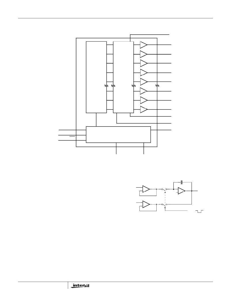
�Block� Diagram�
�REFH�
�OUTA�
�OUTB�
�OUTC�
�OUTD�
�18�
�CHANNEL�
�REGISTERS�
�VOLTAGE�
�SOURCES�
�OUTE�
�OUTP�
�OUTQ�
�OUTR�
�REFL�
�CAP�
�SDI�
�SCLK�
�ENA�
�CONTROL� IF�
�SDO�
�OSC_SELECT�
�EXT_OSC�
�Channel� Outputs�
�Each� of� the� channel� outputs� has� a� rail-to-rail� buffer.� This�
�enables� all� channels� to� have� the� capability� to� drive� to� within�
���Output� Stage� and� the� Use� of� External�
�Oscillator�
�CH�
�When� driving� large� capacitive� loads,� a� series� resistor� should�
�be� placed� in� series� with� the� output.� (Usually� between� 5� Ω� and�
�1.3V�
�+�
�-�
�S� 1�
�1.3V�
�+�
�-�
�V� OUT�
�50� Ω� ).�
�Each� of� the� channels� is� updated� on� a� continuous� cycle,� the�
�time� for� the� new� data� to� appear� at� a� specific� output� will�
�V� IN�
�+�
�-�
�S� 2�
�OSC�
�depend� on� the� exact� timing� relationship� of� the� incoming� data�
�to� this� cycle.�
�The� best-case� scenario� is� when� the� data� has� just� been�
�captured� and� then� passed� on� to� the� output� stage�
�immediately;� this� can� be� as� short� as� 48μs.� In� the� worst-case�
�scenario,� this� will� be� 860μs� for� EL5525,� when� the� data� has�
�just� missed� the� cycle� at� f_OSC� =� 21kHz.�
�When� a� large� change� in� output� voltage� is� required,� the�
�change� will� occur� in� 2V� steps,� thus� the� requisite� number� of�
�timing� cycles� will� be� added� to� the� overall� update� time.� This�
�means� that� a� large� change� of� 16V� can� take� between� 6.8ms�
�and� 7.2ms� depending� on� the� absolute� timing� relative� to� the�
�update� cycle.�
�7�
�FIGURE� 7.� SIMPLIFIED� OUTPUT� SAMPLE� AND� HOLD� AMP�
�STAGE� FOR� ONE� CHANNEL�
�The� output� voltage� is� generated� from� the� DAC,� which� is� V� IN�
�in� Figure� 7.� The� refreshed� switches� are� controlled� by� the�
�internal� or� external� oscillator� signal.� When� the� OSC� clock�
�signal� is� low,� switches� S� 1� and� S� 2� are� closed.� The� output�
�V� OUT� =� V� IN� and� at� the� same� time� the� sample� and� hold� cap�
�CH� is� being� charged.� When� the� OSC� clock� signal� is� high,� the�
�refreshed� switches� S� 1� and� S� 2� are� opened� and� the� output�
�voltage� is� maintained� by� CH.� This� refreshed� process� will�
�repeat� every� 18� clock� cycles� for� each� channel.� The� time�
�FN7393.2�
�September� 21,� 2010�
�相关PDF资料 |
PDF描述 |
|---|---|
| RCM22DTAN-S189 | CONN EDGECARD 44POS R/A .156 SLD |
| EL5525IREZ-T13 | IC VREF GEN 18CH TFTLCD 38HTSSOP |
| X40021V14-CT1 | IC VOLTAGE MONITOR DUAL 14-TSSOP |
| 160USC2200MEFCSN35X40 | CAP ALUM 2200UF 160V 20% SNAP-IN |
| ADP1715ARMZ-1.0-R7 | IC REG LDO 1V .5A 8-MSOP |
相关代理商/技术参数 |
参数描述 |
|---|---|
| EL552-6 | 制造商:未知厂家 制造商全称:未知厂家 功能描述:Logic IC |
| EL552-7 | 制造商:未知厂家 制造商全称:未知厂家 功能描述:Logic IC |
| EL552-8 | 制造商:未知厂家 制造商全称:未知厂家 功能描述:Logic IC |
| EL552-9 | 制造商:未知厂家 制造商全称:未知厂家 功能描述:Logic IC |
| EL553-2.8-0.1 | 制造商:未知厂家 制造商全称:未知厂家 功能描述:Logic IC |
发布紧急采购,3分钟左右您将得到回复。