参数资料
| 型号: | EL7556DCMZ-T13 |
| 厂商: | Intersil |
| 文件页数: | 8/11页 |
| 文件大小: | 0K |
| 描述: | IC REG BUCK SYNC ADJ 6A 28SOIC |
| 标准包装: | 1,000 |
| 类型: | 降压(降压) |
| 输出类型: | 可调式 |
| 输出数: | 1 |
| 输出电压: | 1 V ~ 3.8 V |
| 输入电压: | 5V |
| PWM 型: | 电流模式 |
| 频率 - 开关: | 1MHz |
| 电流 - 输出: | 6A |
| 同步整流器: | 是 |
| 工作温度: | -40°C ~ 85°C |
| 安装类型: | 表面贴装 |
| 封装/外壳: | 28-SOIC(0.295",7.50mm 宽) |
| 包装: | 带卷 (TR) |
| 供应商设备封装: | 28-SOIC W |
�� �
�
�EL7556D�
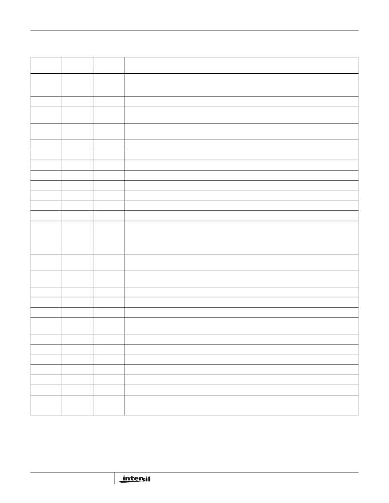
�Pin� Descriptions�
�I� =� Input,� O� =� Output,� S� =� Supply�
�PIN�
�NUMBER�
�1�
�PIN� NAME�
�FB1�
�PIN� TYPE�
�I�
�FUNCTION�
�Voltage� feedback� pin� for� the� buck� regulator.� Active� when� VCC2DET� is� logic� low.� Normally� connected� to�
�external� resistor� divider� between� V� OUT� and� GND.� A� 2μA� pull-up� current� forces� V� OUT� to� V� SS� in� the� event�
�that� FB1� is� floating� and� VCC2DET� is� inadvertently� connected� to� GND.�
�2�
�3�
�CREF�
�CSLOPE�
�I�
�I�
�Bandgap� reference� bypass� capacitor.� Typically� 0.1μF� to� V� SS� .�
�Slope� compensation� capacitor.� Ramp� width� corresponds� to� LX� duty� cycle.� C� SLOPE� to� C� OSC� ratio� is�
�normally� 1:1.5.�
�4�
�COSC�
�I�
�Oscillator� timing� capacitor.� F� OSC� (Hz)� can� be� approximated� by:� F� OSC� (Hz)� =� 0.0001/C� OSC� .� C� OSC� in�
�Farads.�
�5�
�6�
�7�
�8�
�9�
�10�
�11�
�12�
�13�
�VDD�
�VIN�
�VSSP�
�VIN�
�VSSP�
�VSSP�
�VSSP�
�VSSP�
�VCC2DET�
�S�
�S�
�S�
�S�
�S�
�S�
�S�
�S�
�I�
�Power� Supply� for� PWM� control� circuitry.� Normally� the� same� potential� as� V� IN� .�
�Power� supply� for� the� buck� regulator.� Connected� to� the� drain� of� the� high-side� NMOS� FET.�
�Ground� return� for� the� buck� regulator.� Connected� to� the� source� of� the� low-side� synchronous� NMOS� FET.�
�Same� as� pin� 6.�
�Same� as� pin� 7.�
�Same� as� pin� 7.�
�Same� as� pin� 7.�
�Same� as� pin� 7.�
�VCC2DET� interface� logic� input.� When� driven� to� logic� 1� V� OUT� =� 3.500V.� When� driven� to� logic� 0� the� PWM�
�uses� FB1� to� determine� V� OUT� :� V� OUT� =� 1.0V*(1+R3/R4).�
�14�
�OUTEN�
�I�
�The� switching� regulator� output� is� enabled� when� logic� 1.� The� reference� voltage� output� operates� whenever�
�the� power� supply� is� qualified� (V� DD� >VPOR)� regardless� of� the� state� of� this� pin.�
�15�
�OT�
�O�
�Over� temperature� indicator.� Normally� high.� Pulls� low� when� die� temperature� exceeds� 135°C,� returns� to�
�the� high� state� when� die� temperature� has� cooled� to� 100°C.�
�16�
�PWRGD�
�O�
�Power� good� window� comparator� output.� Logic� 1� when� regulator� output� is� within� ±10%� of� programmed�
�voltage.�
�17�
�18�
�19�
�20�
�TEST�
�VSSP�
�VSSP�
�LX�
�I�
�S�
�S�
�O�
�Test� pin.� Must� be� connected� to� VSSP� in� normal� operation.�
�Same� as� pin� 7.�
�Same� as� pin� 7.�
�Inductor� drive� pin.� High� current� switching� output� whose� average� voltage� equals� the� regulator� output�
�voltage.�
�21�
�22�
�23�
�24�
�25�
�26�
�27�
�28�
�LX�
�LX�
�LX�
�VHI�
�VSS�
�C2V�
�CP�
�FB2�
�O�
�O�
�O�
�I�
�S�
�I�
�O�
�I�
�Same� as� pin� 20.�
�Same� as� pin� 20.�
�Same� as� pin� 20.�
�Gate� drive� to� high-side� driver.� Bootstrapped� from� LX� with� a� 0.1μF� capacitor.�
�Ground� return� for� the� control� circuitry.�
�Connected� to� voltage� doubler� output.� Supplies� gate� drive� to� the� low-side� driver.�
�Drives� the� negative� side� of� charge� pump� capacitor� at� one-half� the� oscillator� frequency� F� OSC� .�
�Voltage� feedback� pin.� Active� when� VCC2DET� is� logic� 1.� Internally� preset� to� V� OUT� =� 3.5V.�
�8�
�相关PDF资料 |
PDF描述 |
|---|---|
| EL7562CUZ-T13 | IC REG BUCK SYNC ADJ 2A 16QSOP |
| EL7563CMZ | IC REG BUCK SYNC ADJ 4A 20SOIC |
| EL7564CRE | IC REG BUCK SYNC ADJ 4A 28HTSSOP |
| EL7566DRE-T7 | IC REG BUCK SYNC ADJ 6A 28HTSSOP |
| EL7571CMZ-T13 | IC CTRLR PWM PROGRAMMABLE 20SOIC |
相关代理商/技术参数 |
参数描述 |
|---|---|
| EL7558B | 制造商:INTERSIL 制造商全称:Intersil Corporation 功能描述:Integrated Adjustable 8 Amp Synchronous Switcher |
| EL7558BC | 制造商:ELANTEC 制造商全称:ELANTEC 功能描述:Integrated Adjustable 8 Amp Synchronous Switcher |
| EL7558BCM | 制造商:INTERSIL 制造商全称:Intersil Corporation 功能描述:Integrated Adjustable 8 Amp Synchronous Switcher |
| EL7558BCM-T13 | 制造商:INTERSIL 制造商全称:Intersil Corporation 功能描述:Integrated Adjustable 8 Amp Synchronous Switcher |
| EL7558C | 制造商:未知厂家 制造商全称:未知厂家 功能描述:8 Amp Adjustable CPU Power Supply Unit- Preliminary Data |
发布紧急采购,3分钟左右您将得到回复。