- 您现在的位置:买卖IC网 > PDF目录362734 > EP1C6F144I7ES (Altera Corporation) Cyclone FPGA Family Data Sheet PDF资料下载
参数资料
| 型号: | EP1C6F144I7ES |
| 厂商: | Altera Corporation |
| 英文描述: | Cyclone FPGA Family Data Sheet |
| 中文描述: | 气旋的FPGA系列数据手册 |
| 文件页数: | 39/104页 |
| 文件大小: | 763K |
| 代理商: | EP1C6F144I7ES |
第1页第2页第3页第4页第5页第6页第7页第8页第9页第10页第11页第12页第13页第14页第15页第16页第17页第18页第19页第20页第21页第22页第23页第24页第25页第26页第27页第28页第29页第30页第31页第32页第33页第34页第35页第36页第37页第38页当前第39页第40页第41页第42页第43页第44页第45页第46页第47页第48页第49页第50页第51页第52页第53页第54页第55页第56页第57页第58页第59页第60页第61页第62页第63页第64页第65页第66页第67页第68页第69页第70页第71页第72页第73页第74页第75页第76页第77页第78页第79页第80页第81页第82页第83页第84页第85页第86页第87页第88页第89页第90页第91页第92页第93页第94页第95页第96页第97页第98页第99页第100页第101页第102页第103页第104页
Altera Corporation
January 2007
2–33
Preliminary
Global Clock Network & Phase-Locked Loops
Table 2–6
shows the PLL features in Cyclone devices.
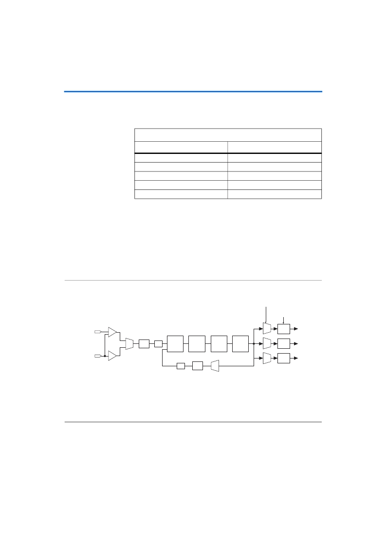
Figure 2–25
shows
a Cyclone PLL.
Figure 2–25. Cyclone PLL
Note (1)
Notes to
Figure 2–25
:
(1)
The EP1C3 device in the 100-pin TQFP package does not support external outputs or LVDS inputs. The EP1C6
device in the 144-pin TQFP package does not support external output from PLL2.
(2)
LVDS input is supported via the secondary function of the dedicated clock pins. For PLL 1, the
CLK0
pin’s secondary
function is
LVDSCLK1p
and the
CLK1
pin’s secondary function is
LVDSCLK1n
. For PLL 2, the
CLK2
pin’s secondary
function is
LVDSCLK2p
and the
CLK3
pin’s secondary function is
LVDSCLK2n
.
(3)
PFD: phase frequency detector.
Table 2–6. Cyclone PLL Features
Feature
PLL Support
Clock multiplication and division
m
/(
n
×
post-scale counter)
(1)
Down to 125-ps increments
(2)
,
(3)
Phase shift
Programmable duty cycle
Yes
N
umber of internal clock outputs
2
N
umber of external clock outputs
One differential or one single-ended
(4)
Notes to
Table 2–6
:
(1)
The
m
counter ranges from 2 to 32. The
n
counter and the post-scale counters
range from 1 to 32.
(2)
The smallest phase shift is determined by the voltage-controlled oscillator (VCO)
period divided by 8.
(3)
For degree increments, Cyclone devices can shift all output frequencies in
increments of 45°. Smaller degree increments are possible depending on the
frequency and divide parameters.
(4)
The EP1C3 device in the 100-pin TQFP package does not support external clock
output. The EP1C6 device in the 144-pin TQFP package does not support external
clock output from PLL2.
Charge
Pump
VCO
PFD
(3)
Loop
Filter
CLK0 or
LVDSCLK1p
(2)
CLK1 or
LVDSCLK1n
(2)
÷
n
÷
m
Δ
t
Δ
t
Global clock
Global clock
I/O buffer
÷g0
÷g1
÷e
VCO Phase Selection
SelecOutput Port
Post-Scale
Counters
相关PDF资料 |
PDF描述 |
|---|---|
| EP1C6F144I8ES | Cyclone FPGA Family Data Sheet |
| EP1C6F240C6ES | Cyclone FPGA Family Data Sheet |
| EP1C6F240C7ES | Cyclone FPGA Family Data Sheet |
| EP1C6F240C8ES | Cyclone FPGA Family Data Sheet |
| EP1C6F240I7ES | Cyclone FPGA Family Data Sheet |
相关代理商/技术参数 |
参数描述 |
|---|---|
| EP1C6F256C6 | 功能描述:FPGA - 现场可编程门阵列 FPGA - Cyclone I 598 LABs 185 IOs RoHS:否 制造商:Altera Corporation 系列:Cyclone V E 栅极数量: 逻辑块数量:943 内嵌式块RAM - EBR:1956 kbit 输入/输出端数量:128 最大工作频率:800 MHz 工作电源电压:1.1 V 最大工作温度:+ 70 C 安装风格:SMD/SMT 封装 / 箱体:FBGA-256 |
| EP1C6F256C6N | 功能描述:FPGA - 现场可编程门阵列 FPGA - Cyclone I 598 LABs 185 IOs RoHS:否 制造商:Altera Corporation 系列:Cyclone V E 栅极数量: 逻辑块数量:943 内嵌式块RAM - EBR:1956 kbit 输入/输出端数量:128 最大工作频率:800 MHz 工作电源电压:1.1 V 最大工作温度:+ 70 C 安装风格:SMD/SMT 封装 / 箱体:FBGA-256 |
| EP1C6F256C7 | 功能描述:FPGA - 现场可编程门阵列 FPGA - Cyclone I 598 LABs 185 IOs RoHS:否 制造商:Altera Corporation 系列:Cyclone V E 栅极数量: 逻辑块数量:943 内嵌式块RAM - EBR:1956 kbit 输入/输出端数量:128 最大工作频率:800 MHz 工作电源电压:1.1 V 最大工作温度:+ 70 C 安装风格:SMD/SMT 封装 / 箱体:FBGA-256 |
| EP1C6F256C7N | 功能描述:FPGA - 现场可编程门阵列 FPGA - Cyclone I 598 LABs 185 IOs RoHS:否 制造商:Altera Corporation 系列:Cyclone V E 栅极数量: 逻辑块数量:943 内嵌式块RAM - EBR:1956 kbit 输入/输出端数量:128 最大工作频率:800 MHz 工作电源电压:1.1 V 最大工作温度:+ 70 C 安装风格:SMD/SMT 封装 / 箱体:FBGA-256 |
| EP1C6F256C8 | 功能描述:FPGA - 现场可编程门阵列 FPGA - Cyclone I 598 LABs 185 IOs RoHS:否 制造商:Altera Corporation 系列:Cyclone V E 栅极数量: 逻辑块数量:943 内嵌式块RAM - EBR:1956 kbit 输入/输出端数量:128 最大工作频率:800 MHz 工作电源电压:1.1 V 最大工作温度:+ 70 C 安装风格:SMD/SMT 封装 / 箱体:FBGA-256 |
发布紧急采购,3分钟左右您将得到回复。