参数资料
| 型号: | EP20K400EFC672-3N |
| 厂商: | Altera |
| 文件页数: | 80/117页 |
| 文件大小: | 0K |
| 描述: | IC APEX 20KE FPGA 400K 672-FBGA |
| 产品培训模块: | Three Reasons to Use FPGA's in Industrial Designs |
| 标准包装: | 40 |
| 系列: | APEX-20K® |
| LAB/CLB数: | 1664 |
| 逻辑元件/单元数: | 16640 |
| RAM 位总计: | 212992 |
| 输入/输出数: | 488 |
| 门数: | 1052000 |
| 电源电压: | 1.71 V ~ 1.89 V |
| 安装类型: | 表面贴装 |
| 工作温度: | 0°C ~ 85°C |
| 封装/外壳: | 672-BBGA |
| 供应商设备封装: | 672-BGA(27x27) |
第1页第2页第3页第4页第5页第6页第7页第8页第9页第10页第11页第12页第13页第14页第15页第16页第17页第18页第19页第20页第21页第22页第23页第24页第25页第26页第27页第28页第29页第30页第31页第32页第33页第34页第35页第36页第37页第38页第39页第40页第41页第42页第43页第44页第45页第46页第47页第48页第49页第50页第51页第52页第53页第54页第55页第56页第57页第58页第59页第60页第61页第62页第63页第64页第65页第66页第67页第68页第69页第70页第71页第72页第73页第74页第75页第76页第77页第78页第79页当前第80页第81页第82页第83页第84页第85页第86页第87页第88页第89页第90页第91页第92页第93页第94页第95页第96页第97页第98页第99页第100页第101页第102页第103页第104页第105页第106页第107页第108页第109页第110页第111页第112页第113页第114页第115页第116页第117页
Altera Corporation
65
APEX 20K Programmable Logic Device Family Data Sheet
1
For DC Operating Specifications on APEX 20KE I/O standards,
please refer to Application Note 117 (Using Selectable I/O Standards
in Altera Devices).
(1)
See the Operating Requirements for Altera Devices Data Sheet.
(2)
Minimum DC input is –0.5 V. During transitions, the inputs may undershoot to –2.0 V or overshoot to 5.75 V for
input currents less than 100 mA and periods shorter than 20 ns.
(3)
Numbers in parentheses are for industrial-temperature-range devices.
(4)
Maximum VCC rise time is 100 ms, and VCC must rise monotonically.
(5)
Minimum DC input is –0.5 V. During transitions, the inputs may undershoot to –2.0 V or overshoot to the voltage
shown in the following table based on input duty cycle for input currents less than 100 mA. The overshoot is
dependent upon duty cycle of the signal. The DC case is equivalent to 100% duty cycle.
Vin
Max. Duty Cycle
4.0V
100% (DC)
4.1
90%
4.2
50%
4.3
30%
4.4
17%
4.5
10%
(6)
All pins, including dedicated inputs, clock, I/O, and JTAG pins, may be driven before VCCINT and VCCIO are
powered.
(7)
Typical values are for TA = 25° C, VCCINT = 1.8 V, and VCCIO = 1.8 V, 2.5 V or 3.3 V.
(8)
These values are specified under the APEX 20KE device recommended operating conditions, shown in Table 24 on
(9)
Refer to Application Note 117 (Using Selectable I/O Standards in Altera Devices) for the VIH, VIL, VOH, VOL, and II
parameters when VCCIO = 1.8 V.
(10) The APEX 20KE input buffers are compatible with 1.8-V, 2.5-V and 3.3-V (LVTTL and LVCMOS) signals.
Additionally, the input buffers are 3.3-V PCI compliant. Input buffers also meet specifications for GTL+, CTT, AGP,
SSTL-2, SSTL-3, and HSTL.
(11) The IOH parameter refers to high-level TTL, PCI, or CMOS output current.
(12) The IOL parameter refers to low-level TTL, PCI, or CMOS output current. This parameter applies to open-drain pins
as well as output pins.
(13) This value is specified for normal device operation. The value may vary during power-up.
(14) Pin pull-up resistance values will be lower if an external source drives the pin higher than VCCIO.
(15) Capacitance is sample-tested only.
compliance on APEX 20K devices.
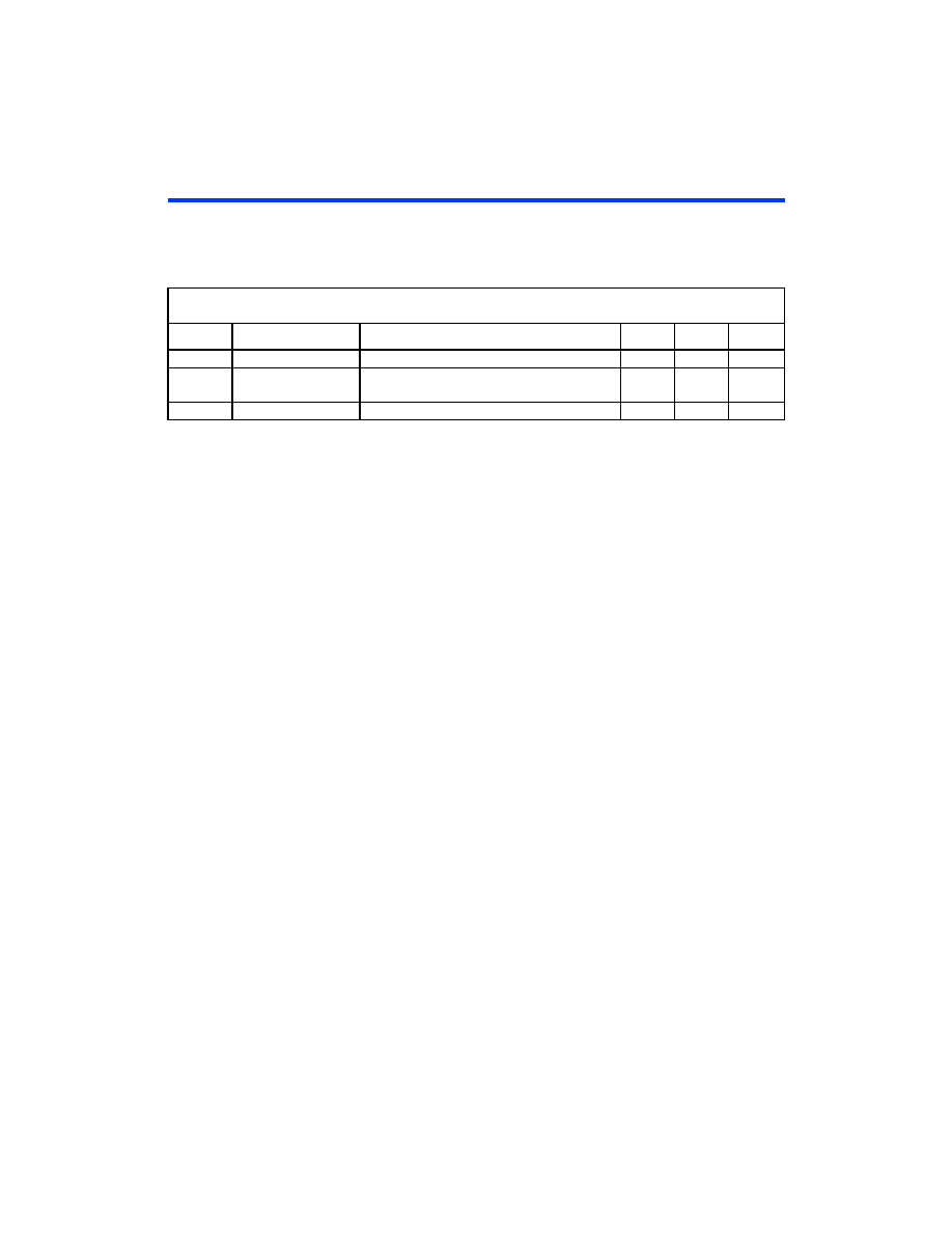
Table 30. APEX 20KE Device Capacitance
Symbol
Parameter
Conditions
Min
Max
Unit
CIN
Input capacitance
VIN = 0 V, f = 1.0 MHz
8
pF
CINCLK
Input capacitance on
dedicated clock pin
VIN = 0 V, f = 1.0 MHz
12
pF
COUT
Output capacitance
VOUT = 0 V, f = 1.0 MHz
8
pF
相关PDF资料 |
PDF描述 |
|---|---|
| EP20K400EFC672-3 | IC APEX 20KE FPGA 400K 672-FBGA |
| IDT70V25L20PFI | IC SRAM 128KBIT 20NS 100TQFP |
| ACM44DRAN | CONN EDGECARD 88POS .156 R/A |
| A54SX16P-PQ208M | IC FPGA SX 24K GATES 208-PQFP |
| A54SX16P-PQG208M | IC FPGA SX 24K GATES 208-PQFP |
相关代理商/技术参数 |
参数描述 |
|---|---|
| EP20K400EFI672-1ES | 制造商:未知厂家 制造商全称:未知厂家 功能描述:FPGA |
| EP20K400EFI672-2ES | 制造商:未知厂家 制造商全称:未知厂家 功能描述:FPGA |
| EP20K400EFI672-2N | 功能描述:FPGA - 现场可编程门阵列 CPLD - APEX 20K 1664 Macros 488 IO RoHS:否 制造商:Altera Corporation 系列:Cyclone V E 栅极数量: 逻辑块数量:943 内嵌式块RAM - EBR:1956 kbit 输入/输出端数量:128 最大工作频率:800 MHz 工作电源电压:1.1 V 最大工作温度:+ 70 C 安装风格:SMD/SMT 封装 / 箱体:FBGA-256 |
| EP20K400EFI672-2X | 功能描述:FPGA - 现场可编程门阵列 CPLD - APEX 20K 1664 Macros 488 IO RoHS:否 制造商:Altera Corporation 系列:Cyclone V E 栅极数量: 逻辑块数量:943 内嵌式块RAM - EBR:1956 kbit 输入/输出端数量:128 最大工作频率:800 MHz 工作电源电压:1.1 V 最大工作温度:+ 70 C 安装风格:SMD/SMT 封装 / 箱体:FBGA-256 |
| EP20K400EFI672-3ES | 制造商:未知厂家 制造商全称:未知厂家 功能描述:FPGA |
发布紧急采购,3分钟左右您将得到回复。