- 您现在的位置:买卖IC网 > PDF目录97921 > EP20K400FC672-3ES FPGA PDF资料下载
参数资料
| 型号: | EP20K400FC672-3ES |
| 英文描述: | FPGA |
| 中文描述: | FPGA的 |
| 文件页数: | 41/114页 |
| 文件大小: | 1623K |
| 代理商: | EP20K400FC672-3ES |
第1页第2页第3页第4页第5页第6页第7页第8页第9页第10页第11页第12页第13页第14页第15页第16页第17页第18页第19页第20页第21页第22页第23页第24页第25页第26页第27页第28页第29页第30页第31页第32页第33页第34页第35页第36页第37页第38页第39页第40页当前第41页第42页第43页第44页第45页第46页第47页第48页第49页第50页第51页第52页第53页第54页第55页第56页第57页第58页第59页第60页第61页第62页第63页第64页第65页第66页第67页第68页第69页第70页第71页第72页第73页第74页第75页第76页第77页第78页第79页第80页第81页第82页第83页第84页第85页第86页第87页第88页第89页第90页第91页第92页第93页第94页第95页第96页第97页第98页第99页第100页第101页第102页第103页第104页第105页第106页第107页第108页第109页第110页第111页第112页第113页第114页
32
Altera Corporation
APEX 20K Programmable Logic Device Family Data Sheet
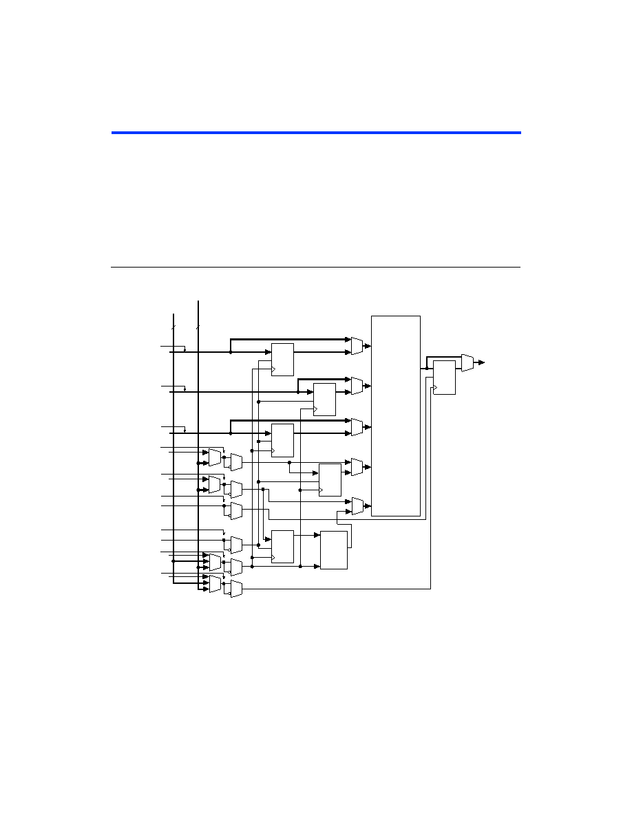
Read/Write Clock Mode
The read/write clock mode contains two clocks. One clock controls all
registers associated with writing: data input, WE, and write address. The
other clock controls all registers associated with reading: read enable
(RE), read address, and data output. The ESB also supports clock enable
and asynchronous clear signals; these signals also control the read and
write registers independently. Read/write clock mode is commonly used
for applications where reads and writes occur at different system
frequencies. Figure 20 shows the ESB in read/write clock mode.
Figure 20. ESB in Read/Write Clock Mode
Notes:
(1)
All registers can be cleared asynchronously by ESB local interconnect signals, global signals, or the chip-wide reset.
(2)
APEX 20KE devices have four dedicated clocks.
Dedicated Clocks
2 or 4
4
D
ENA
Q
D
ENA
Q
D
ENA
Q
D
ENA
Q
D
ENA
Q
data[ ]
rdaddress[ ]
wraddress[ ]
RAM/ROM
128
× 16
256
× 8
512
× 4
1,024
× 2
2,048
× 1
Data In
Read Address
Write Address
Read Enable
Write Enable
Data Out
outclken
inclken
inclock
outclock
D
ENA
Q
Write
Pulse
Generator
rden
wren
Dedicated Inputs &
Global Signals
to MegaLAB,
FastTrack &
Local
Interconnect
(2)
相关PDF资料 |
PDF描述 |
|---|---|
| EP20K400FI672-1 | Field Programmable Gate Array (FPGA) |
| EP20K400FI672-1ES | FPGA |
| EP20K400FI672-2 | Field Programmable Gate Array (FPGA) |
| EP20K100QC240-3ES | Boost + VON Slice + VCOM; Temperature Range: -40°C to 85°C; Package: 24-QFN T&R |
| EP20K100QI208-1 | Boost + LDO + VON Slice + VCOM; Temperature Range: -40°C to 85°C; Package: 24-QFN T&R |
相关代理商/技术参数 |
参数描述 |
|---|---|
| EP20K400FC672-3V | 制造商:Rochester Electronics LLC 功能描述:- Bulk |
| EP20K400FI672-1 | 制造商:未知厂家 制造商全称:未知厂家 功能描述:Field Programmable Gate Array (FPGA) |
| EP20K400FI672-1ES | 制造商:未知厂家 制造商全称:未知厂家 功能描述:FPGA |
| EP20K400FI672-2 | 制造商:未知厂家 制造商全称:未知厂家 功能描述:Field Programmable Gate Array (FPGA) |
| EP20K400FI672-2ES | 制造商:未知厂家 制造商全称:未知厂家 功能描述:FPGA |
发布紧急采购,3分钟左右您将得到回复。