参数资料
| 型号: | EP2AGX65DF25C6N |
| 厂商: | Altera |
| 文件页数: | 13/90页 |
| 文件大小: | 0K |
| 描述: | IC ARRIA II GX FPGA 65K 572FBGA |
| 产品培训模块: | Three Reasons to Use FPGA's in Industrial Designs |
| 标准包装: | 5 |
| 系列: | Arria II GX |
| LAB/CLB数: | 2530 |
| 逻辑元件/单元数: | 60214 |
| RAM 位总计: | 5371904 |
| 输入/输出数: | 252 |
| 电源电压: | 0.87 V ~ 0.93 V |
| 安装类型: | 表面贴装 |
| 工作温度: | 0°C ~ 85°C |
| 封装/外壳: | 572-FBGA |
| 供应商设备封装: | 572-FBGA |
第1页第2页第3页第4页第5页第6页第7页第8页第9页第10页第11页第12页当前第13页第14页第15页第16页第17页第18页第19页第20页第21页第22页第23页第24页第25页第26页第27页第28页第29页第30页第31页第32页第33页第34页第35页第36页第37页第38页第39页第40页第41页第42页第43页第44页第45页第46页第47页第48页第49页第50页第51页第52页第53页第54页第55页第56页第57页第58页第59页第60页第61页第62页第63页第64页第65页第66页第67页第68页第69页第70页第71页第72页第73页第74页第75页第76页第77页第78页第79页第80页第81页第82页第83页第84页第85页第86页第87页第88页第89页第90页
1–12
Chapter 1: Device Datasheet for Arria II Devices
Electrical Characteristics
December 2013
Altera Corporation
Use the following with Equation 1–1:
■
RSCAL is the OCT resistance value at power up.
■
T is the variation of temperature with respect to the temperature at power up.
■
V is the variation of voltage with respect to the VCCIO at power up.
■
dR/dT is the percentage change of RSCAL with temperature.
■
dR/dV is the percentage change of RSCAL with voltage.
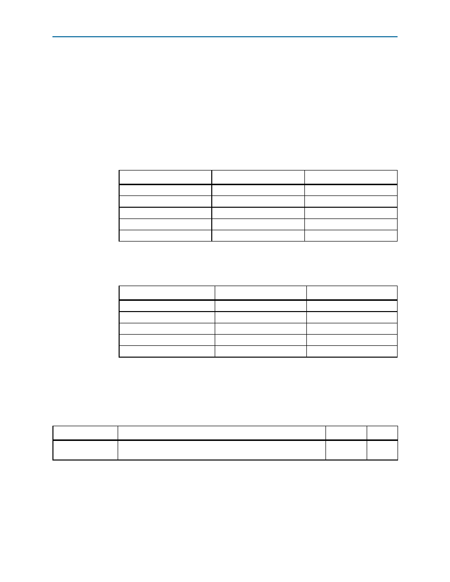
Table 1–14 lists the OCT variation with temperature and voltage after power-up
calibration for Arria II GX devices.
Table 1–15 lists the OCT variation with temperature and voltage after power-up
calibration for Arria II GZ devices.
Pin Capacitance
Table 1–16 lists the pin capacitance for Arria II GX devices.
Table 1–14. OCT Variation after Power-up Calibration for Arria II GX Devices
Nominal Voltage VCCIO (V)
dR/dT (%/°C)
dR/dV (%/mV)
3.0
0.262
0.035
2.5
0.234
0.039
1.8
0.219
0.086
1.5
0.199
0.136
1.2
0.161
0.288
Table 1–15. OCT Variation after Power-Up Calibration for Arria II GZ Devices (Note 1)
Nominal Voltage, V
CCIO (V)
dR/dT (%/°C)
dR/dV (%/mV)
3.0
0.189
0.0297
2.5
0.208
0.0344
1.8
0.266
0.0499
1.5
0.273
0.0744
1.2
0.317
0.1241
Note to Table 1–15:
(1) Valid for VCCIO range of ±5% and temperature range of 0° to 85°C.
Table 1–16. Pin Capacitance for Arria II GX Devices
Symbol
Description
Typical
Unit
CIO
Input capacitance on I/O pins, dual-purpose pins (differential I/O, clock,
Rup, Rdn), and dedicated clock input pins
7pF
相关PDF资料 |
PDF描述 |
|---|---|
| ABB80DHFR | CONN EDGECARD 160POS .050 SMD |
| A42MX36-1BG272I | IC FPGA MX SGL CHIP 54K 272-PBGA |
| A42MX36-1BGG272I | IC FPGA MX SGL CHIP 54K 272-PBGA |
| EP20K400EFC672-3N | IC APEX 20KE FPGA 400K 672-FBGA |
| EP20K400EFC672-3 | IC APEX 20KE FPGA 400K 672-FBGA |
相关代理商/技术参数 |
参数描述 |
|---|---|
| EP2AGX65DF25C6NES | 制造商:Altera Corporation 功能描述:FPGA Arria 制造商:Altera Corporation 功能描述:FPGA Arria? II GX Family 60214 Cells 400MHz 40nm Technology 0.9V 572-Pin FC-FBGA 制造商:Altera Corporation 功能描述:IC ARRIA II GX FPGA 572FBGA |
| EP2AGX65DF25I3 | 功能描述:IC ARRIA II GX FPGA 65K 572FBGA RoHS:否 类别:集成电路 (IC) >> 嵌入式 - FPGA(现场可编程门阵列) 系列:Arria II GX 产品变化通告:XC4000(E,L) Discontinuation 01/April/2002 标准包装:24 系列:XC4000E/X LAB/CLB数:100 逻辑元件/单元数:238 RAM 位总计:3200 输入/输出数:80 门数:3000 电源电压:4.5 V ~ 5.5 V 安装类型:表面贴装 工作温度:-40°C ~ 100°C 封装/外壳:120-BCBGA 供应商设备封装:120-CPGA(34.55x34.55) |
| EP2AGX65DF25I3N | 功能描述:FPGA - 现场可编程门阵列 FPGA - Arria II GX 2530 LABs 252 IOs RoHS:否 制造商:Altera Corporation 系列:Cyclone V E 栅极数量: 逻辑块数量:943 内嵌式块RAM - EBR:1956 kbit 输入/输出端数量:128 最大工作频率:800 MHz 工作电源电压:1.1 V 最大工作温度:+ 70 C 安装风格:SMD/SMT 封装 / 箱体:FBGA-256 |
| EP2AGX65DF25I5 | 功能描述:FPGA - 现场可编程门阵列 FPGA - Arria II GX 2530 LABs 252 IOs RoHS:否 制造商:Altera Corporation 系列:Cyclone V E 栅极数量: 逻辑块数量:943 内嵌式块RAM - EBR:1956 kbit 输入/输出端数量:128 最大工作频率:800 MHz 工作电源电压:1.1 V 最大工作温度:+ 70 C 安装风格:SMD/SMT 封装 / 箱体:FBGA-256 |
| EP2AGX65DF25I5N | 功能描述:FPGA - 现场可编程门阵列 FPGA - Arria II GX 2530 LABs 252 IOs RoHS:否 制造商:Altera Corporation 系列:Cyclone V E 栅极数量: 逻辑块数量:943 内嵌式块RAM - EBR:1956 kbit 输入/输出端数量:128 最大工作频率:800 MHz 工作电源电压:1.1 V 最大工作温度:+ 70 C 安装风格:SMD/SMT 封装 / 箱体:FBGA-256 |
发布紧急采购,3分钟左右您将得到回复。