- 您现在的位置:买卖IC网 > PDF目录16863 > EV-ADF4360-4EB1Z (Analog Devices Inc)BOARD EVAL FOR ADF4360-4 PDF资料下载
参数资料
| 型号: | EV-ADF4360-4EB1Z |
| 厂商: | Analog Devices Inc |
| 文件页数: | 14/24页 |
| 文件大小: | 0K |
| 描述: | BOARD EVAL FOR ADF4360-4 |
| 标准包装: | 1 |
| 主要目的: | 计时,频率合成器 |
| 嵌入式: | 否 |
| 已用 IC / 零件: | ADF4360-4 |
| 主要属性: | 带 VCO 的单路整数-N PLL |
| 次要属性: | 1.6GHz,200kHz PFD |
| 已供物品: | 板,缆线,CD |
| 其它名称: | Q7037782 |
Data Sheet
ADF4360-4
Rev. B | Page 21 of 24
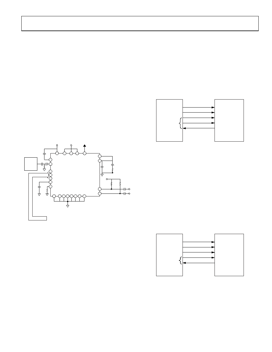
FIXED FREQUENCY LO
Figure 18 shows the ADF4360-4 used as a fixed frequency LO at
1.6 GHz. The low-pass filter was designed using ADIsimPLL for
a channel spacing of 8 MHz and an open-loop bandwidth of
40 kHz. The maximum PFD frequency of the ADF4360-4 is
8 MHz. Because using a larger PFD frequency allows users to
use a smaller N, the in-band phase noise is reduced to as low as
possible, –100 dBc/Hz. The 40 kHz bandwidth is chosen to be
just greater than the point at which the open-loop phase noise
of the VCO is –100 dBc/Hz, thus giving the best possible inte-
grated noise. The typical rms phase noise (100 Hz to 100 kHz)
of the LO in this configuration is 0.3°. The reference frequency
is from a 16 MHz TCXO from Fox; thus, an R value of 2 is pro-
grammed. Taking into account the high PFD frequency and its
effect on the band select logic, the band select clock divider is
enabled. In this case, a value of 8 is chosen. A very simple pull-
up resistor and dc blocking capacitor complete the RF output
stage.
SPI
COMPATIBLE
SERIAL
BUS
ADF4360-4
VVCO
FOX
801BE-160
16MHz
VVCO
CPGND
AGND
DGND RF
OUTB
RFOUTA
CP
1nF
4.7nF
22.0nF
51
51
51
100pF
1nF
10
F
4.7k
430
RSET
CC
LE
DATA
CLK
REFIN
CN
VTUNE
DVDD AVDD CE MUXOUT
5
4
24
7
20
23
2
21
6
14
16
17
18
19
13
1
3
8
9
10
11
22
15
12
VVDD
LOCK
DETECT
04438-022
Figure 18. Fixed Frequency LO
INTERFACING
The ADF4360 family has a simple SPI-compatible serial inter-
face for writing to the device. CLK, DATA, and LE control the
data transfer. When LE goes high, the 24 bits that have been
clocked into the appropriate register on each rising edge of CLK
are transferred to the appropriate latch. See Figure 2 for the
timing diagram and Table 5 for the latch truth table.
The maximum allowable serial clock rate is 20 MHz. This
means that the maximum update rate possible is 833 kHz or
one update every 1.2 s. This is certainly more than adequate
for systems that have typical lock times in hundreds of micro-
seconds.
ADuC812 Interface
Figure 19 shows the interface between the ADF4360 family and
the ADuC812 MicroConverter. Because the ADuC812 is based
on an 8051 core, this interface can be used with any 8051-based
microcontroller. The MicroConverter is set up for SPI master
mode with CPHA = 0. To initiate the operation, the I/O port
driving LE is brought low. Each latch of the ADF4360 family
needs a 24-bit word, which is accomplished by writing three
8-bit bytes from the MicroConverter to the device. When the
third byte is written, the LE input should be brought high to
complete the transfer.
04438-023
ADuC812
ADF4360-x
SCLK
SDATA
LE
CE
MUXOUT
(LOCK DETECT)
SCLOCK
MOSI
I/O PORTS
Figure 19. ADuC812 to ADF4360-x Interface
I/O port lines on the ADuC812 are also used to control pow-
erdown (CE input) and detect lock (MUXOUT configured as
lock detect and polled by the port input). When operating in
the described mode, the maximum SCLOCK rate of the
ADuC812 is 4 MHz. This means that the maximum rate at
which the output frequency can be changed is 166 kHz.
ADSP-21xx Interface
Figure 20 shows the interface between the ADF4360 family and
the ADSP-21xx digital signal processor. The ADF4360 family
needs a 24-bit serial word for each latch write. The easiest way
to accomplish this using the ADSP-21xx family is to use the
autobuffered transmit mode of operation with alternate fram-
ing. This provides a means for transmitting an entire block of
serial data before an interrupt is generated.
04438-024
ADSP-21xx
ADF4360-x
SCLK
SDATA
LE
CE
MUXOUT
(LOCK DETECT)
SCLOCK
MOSI
TFS
I/O PORTS
Figure 20. ADSP-21xx to ADF4360-x Interface
Set up the word length for 8 bits and use three memory loca-
tions for each 24-bit word. To program each 24-bit latch, store
the 8-bit bytes, enable the autobuffered mode, and write to the
transmit register of the DSP. This last operation initiates the
autobuffer transfer.
相关PDF资料 |
PDF描述 |
|---|---|
| V110B15E150BF2 | CONVERTER MOD DC/DC 15V 150W |
| GEC31DRXH-S734 | CONN EDGECARD 62POS DIP .100 SLD |
| TAT-125-1/4-0-STK | HEATSHRINK DUAL WALL 1/4"X4' BLK |
| AFK157M35F24T-F | CAP ALUM 150UF 35V 20% SMD |
| SRR7032-681M | INDUCTOR POWER 680UH .16A SMD |
相关代理商/技术参数 |
参数描述 |
|---|---|
| EV-ADF4360-5EB1Z | 功能描述:时钟和定时器开发工具 Evaluation Board I.C. RoHS:否 制造商:Texas Instruments 产品:Evaluation Modules 类型:Clock Conditioners 工具用于评估:LMK04100B 频率:122.8 MHz 工作电源电压:3.3 V |
| EV-ADF4360-6EB1Z | 功能描述:BOARD EVAL FOR ADS4360-6EBIZ RoHS:否 类别:编程器,开发系统 >> 评估演示板和套件 系列:* 标准包装:1 系列:- 主要目的:电信,线路接口单元(LIU) 嵌入式:- 已用 IC / 零件:IDT82V2081 主要属性:T1/J1/E1 LIU 次要属性:- 已供物品:板,电源,线缆,CD 其它名称:82EBV2081 |
| EV-ADF4360-7EB1Z | 功能描述:BOARD EVAL FOR ADF4360-7 RoHS:是 类别:编程器,开发系统 >> 评估演示板和套件 系列:- 标准包装:1 系列:- 主要目的:电信,线路接口单元(LIU) 嵌入式:- 已用 IC / 零件:IDT82V2081 主要属性:T1/J1/E1 LIU 次要属性:- 已供物品:板,电源,线缆,CD 其它名称:82EBV2081 |
| EV-ADF4360-8EB1Z | 功能描述:BOARD EVALUATION FOR ADF4360-8 RoHS:是 类别:编程器,开发系统 >> 评估演示板和套件 系列:- 标准包装:1 系列:- 主要目的:电信,线路接口单元(LIU) 嵌入式:- 已用 IC / 零件:IDT82V2081 主要属性:T1/J1/E1 LIU 次要属性:- 已供物品:板,电源,线缆,CD 其它名称:82EBV2081 |
| EV-ADF4360-9EB1Z | 功能描述:BOARD EVAL FOR ADF4360-9 RoHS:是 类别:编程器,开发系统 >> 评估演示板和套件 系列:- 标准包装:1 系列:- 主要目的:电信,线路接口单元(LIU) 嵌入式:- 已用 IC / 零件:IDT82V2081 主要属性:T1/J1/E1 LIU 次要属性:- 已供物品:板,电源,线缆,CD 其它名称:82EBV2081 |
发布紧急采购,3分钟左右您将得到回复。