- 您现在的位置:买卖IC网 > PDF目录16593 > EVAL-AD5235SDZ (Analog Devices Inc)BOARD EVAL FOR AD5235 PDF资料下载
参数资料
| 型号: | EVAL-AD5235SDZ |
| 厂商: | Analog Devices Inc |
| 文件页数: | 17/32页 |
| 文件大小: | 0K |
| 描述: | BOARD EVAL FOR AD5235 |
| 标准包装: | 1 |
| 主要目的: | 数字电位器 |
| 嵌入式: | 否 |
| 已用 IC / 零件: | AD5235 |
| 主要属性: | 2 沟道,1024 位置 |
| 次要属性: | SPI 接口 |
| 已供物品: | 板,CD |
第1页第2页第3页第4页第5页第6页第7页第8页第9页第10页第11页第12页第13页第14页第15页第16页当前第17页第18页第19页第20页第21页第22页第23页第24页第25页第26页第27页第28页第29页第30页第31页第32页
AD5235
Data Sheet
Rev. F | Page 24 of 32
APPLICATIONS INFORMATION
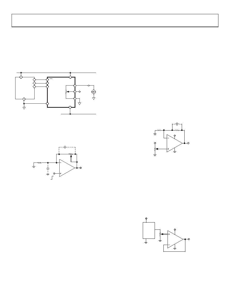
BIPOLAR OPERATION FROM DUAL SUPPLIES
The AD5235 can be operated from ±2.5 V dual supplies, which
enable control of ground referenced ac signals or bipolar operation.
AC signals as high as VDD and VSS can be applied directly across
Terminal A to Terminal B with the output taken from Terminal W.
See Figure 47 for a typical circuit connection.
±2.5V p-p
AD5235
VSS
GND
SDI
CLK
SS
SCLK
MOSI
GND
VDD
MICRO-
CONTROLLER
±1.25V p-p
VDD
+2.5V
–2.5V
CS
D = MIDSCALE
A
W
B
02816-
046
Figure 47. Bipolar Operation from Dual Supplies
GAIN CONTROL COMPENSATION
A digital potentiometer is commonly used in gain control such
as the noninverting gain amplifier shown in Figure 48.
U1
VO
R2
02816-
047
250k
VI
R1
47k
C1
11pF
W
B
A
C2
2.2pF
Figure 48. Typical Noninverting Gain Amplifier
When the RDAC B terminal parasitic capacitance is connected
to the op amp noninverting node, it introduces a zero for the 1/βO
term with 20 dB/dec, whereas a typical op amp gain bandwidth
product (GBP) has 20 dB/dec characteristics. A large R2 and
finite C1 can cause the frequency of this zero to fall well below
the crossover frequency. Therefore, the rate of closure becomes
40 dB/dec, and the system has a 0° phase margin at the crossover
frequency. If an input is a rectangular pulse or step function, the
output can ring or oscillate. Similarly, it is also likely to ring when
switching between two gain values; this is equivalent to a stop
change at the input.
Depending on the op amp GBP, reducing the feedback resistor
might extend the frequency of the zero far enough to overcome
the problem. A better approach is to include a compensation
capacitor, C2, to cancel the effect caused by C1. Optimum
compensation occurs when R1 × C1 = R2 × C2. This is not
an option because of the variation of R2. As a result, one can
use the previous relationship and scale C2 as if R2 were at its
maximum value. Doing this might overcompensate and
compromise the performance when R2 is set at low values.
Alternatively, it avoids the ringing or oscillation at the worst
case. For critical applications, find C2 empirically to suit the
oscillation. In general, C2 in the range of a few picofarads to
no more than a few tenths of picofarads is usually adequate
for the compensation.
Similarly, W and A terminal capacitances are connected to the
output (not shown); their effect at this node is less significant
and the compensation can be avoided in most cases.
HIGH VOLTAGE OPERATION
The digital potentiometer can be placed directly in the feedback or
input path of an op amp for gain control, provided that the voltage
across Terminal A to Terminal B, Terminal W to Terminal A or
Terminal W to Terminal B does not exceed |5 V|. When high
voltage gain is needed, set a fixed gain in the op amp and let the
digital potentiometer control the adjustable input. Figure 49
shows a simple implementation.
2R
R
VO
A1
V+
V–
15V
0V TO 15V
02816-
048
C
A
B
W
AD5235
5V
Figure 49. 15 V Voltage Span Control
Similarly, a compensation capacitor, C, may be needed to dampen
the potential ringing when the digital potentiometer changes
steps. This effect is prominent when stray capacitance at the
inverted node is augmented by a large feedback resistor. Typically,
a picofarad Capacitor C is adequate to combat the problem.
DAC
For DAC operation (see Figure 50), it is common to buffer the
output of the digital potentiometer unless the load is much larger
than RWB. The buffer serves the purpose of impedance
conversion and can drive heavier loads.
AD8601
V+
V–
5V
VO
A1
02816-
049
AD1582
GND
VIN
VOUT
3
2
5V
U1
1
AD5235
A
B
W
Figure 50. Unipolar 10-Bit DAC
相关PDF资料 |
PDF描述 |
|---|---|
| MCZ33742EGR2 | IC SYSTEM BASIS CHIP CAN 28-SOIC |
| ECM30DCAN | CONN EDGECARD 60POS R/A .156 SLD |
| EVAL-ADCMP561BRQZ | BOARD EVALUATION ADCMP561BRQZ |
| VI-BNB-EW | CONVERTER MOD DC/DC 95V 100W |
| A3AAB-2036M | IDC CABLE- ASC20B/AE20M/ASC20B |
相关代理商/技术参数 |
参数描述 |
|---|---|
| EVAL-AD5235SDZ | 制造商:Analog Devices 功能描述:Evaluation board |
| EVAL-AD5242EBZ | 功能描述:BOARD EVALUATION FOR AD5242 RoHS:是 类别:编程器,开发系统 >> 评估演示板和套件 系列:- 标准包装:1 系列:- 主要目的:电信,线路接口单元(LIU) 嵌入式:- 已用 IC / 零件:IDT82V2081 主要属性:T1/J1/E1 LIU 次要属性:- 已供物品:板,电源,线缆,CD 其它名称:82EBV2081 |
| EVAL-AD5243SDZ | 功能描述:BOARD EVAL FOR AD5243 RoHS:是 类别:编程器,开发系统 >> 评估演示板和套件 系列:* 标准包装:1 系列:- 主要目的:电信,线路接口单元(LIU) 嵌入式:- 已用 IC / 零件:IDT82V2081 主要属性:T1/J1/E1 LIU 次要属性:- 已供物品:板,电源,线缆,CD 其它名称:82EBV2081 |
| EVAL-AD5245EBZ | 功能描述:EVAL BOARD FOR AD5245 RoHS:是 类别:编程器,开发系统 >> 评估演示板和套件 系列:- 标准包装:1 系列:- 主要目的:电信,线路接口单元(LIU) 嵌入式:- 已用 IC / 零件:IDT82V2081 主要属性:T1/J1/E1 LIU 次要属性:- 已供物品:板,电源,线缆,CD 其它名称:82EBV2081 |
| EVAL-AD5246DBZ | 功能描述:BOARD EVAL FOR AD5246DBZ RoHS:否 类别:编程器,开发系统 >> 评估演示板和套件 系列:* 标准包装:1 系列:- 主要目的:电信,线路接口单元(LIU) 嵌入式:- 已用 IC / 零件:IDT82V2081 主要属性:T1/J1/E1 LIU 次要属性:- 已供物品:板,电源,线缆,CD 其它名称:82EBV2081 |
发布紧急采购,3分钟左右您将得到回复。