- 您现在的位置:买卖IC网 > PDF目录17075 > EVAL-AD5361EBZ (Analog Devices Inc)BOARD EVAL FOR AD5361 PDF资料下载
参数资料
| 型号: | EVAL-AD5361EBZ |
| 厂商: | Analog Devices Inc |
| 文件页数: | 10/29页 |
| 文件大小: | 0K |
| 描述: | BOARD EVAL FOR AD5361 |
| 产品培训模块: | DAC Architectures |
| 标准包装: | 1 |
| DAC 的数量: | 16 |
| 位数: | 14 |
| 采样率(每秒): | 540k |
| 数据接口: | 串行 |
| 设置时间: | 20µs |
| DAC 型: | 电压 |
| 工作温度: | -40°C ~ 85°C |
| 已供物品: | 板,CD |
| 已用 IC / 零件: | AD5361 |
| 相关产品: | AD5361BSTZ-REEL-ND - IC DAC 14BIT 16CH SERIAL 52-LQFP AD5361BSTZ-ND - IC DAC 14BIT 16CH SERIAL 56LQFP AD5361BCPZ-REEL7-ND - IC DAC 14BIT 16CH SERIAL 56LFCSP AD5361BCPZ-ND - IC DAC 14BIT 16CH SERIAL 56LFCSP |
第1页第2页第3页第4页第5页第6页第7页第8页第9页当前第10页第11页第12页第13页第14页第15页第16页第17页第18页第19页第20页第21页第22页第23页第24页第25页第26页第27页第28页第29页
AD5360/AD5361
Rev. A | Page 17 of 28
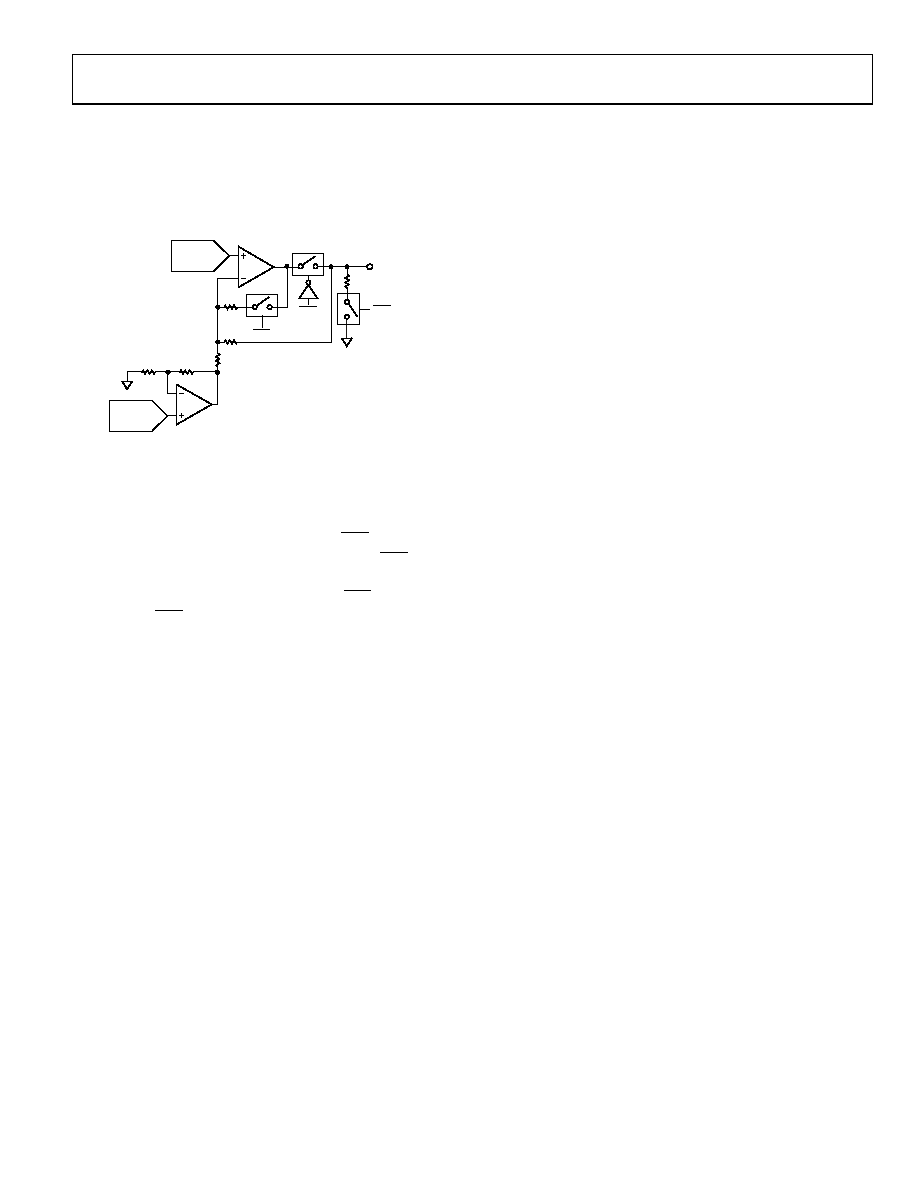
OUTPUT AMPLIFIER
Because the output amplifiers can swing to 1.4 V below the
positive supply and 1.4 V above the negative supply, this limits
how much the output can be offset for a given reference voltage.
For example, it is not possible to have a unipolar output range of
20 V because the maximum supply voltage is ±16.5 V.
CLR
DAC
CHANNEL
OFFSET
DAC
OUTPUT
R6
10k
R2
20k
S3
S2
S1
R4
60k
R3
20k
SIGGND
R5
60k
R1
20k
05
76
1-
0
06
Figure 23. Output Amplifier and Offset DAC
Figure 23 shows details of a DAC output amplifier and its
connections to the offset DAC. On power-up, S1 is open,
disconnecting the amplifier from the output. S3 is closed, so
the output is pulled to SIGGND. S2 is also closed to prevent
the output amplifier from being open-loop. If CLR is low at
power-up, the output remains in this condition until CLR is
taken high. The DAC registers can be programmed, and the
outputs assume the programmed values when CLR is taken
high. Even if CLR is high at power-up, the output remains
in this condition until VDD > 6 V and VSS < 4 V and the
initialization sequence has finished. The outputs then go to
their power-on default values.
TRANSFER FUNCTION
The output voltage of a DAC in the AD5360/AD5361 is dependent
on the value in the input register, the value of the M and C
registers, and the value in the offset DAC. The transfer functions
for the AD5360/AD5361 are shown in the following sections.
AD5360 Transfer Function
The input code is the value in the X1A or X1B register that is
applied to DAC (X1A, X1B default code = 32,768)
DAC_CODE = INPUT_CODE × (M + 1)/216 + C 215
DAC output voltage
VOUT = 4 × VREF × (DAC_CODE (OFFSET_CODE × 4))/
216 + VSIGGND
where:
DAC_CODE should be within the range of 0 to 65,535.
VREF = 3.0 V, for a 12 V span.
VREF = 5.0 V, for a 20 V span.
M = code in gain register default code = 216 – 1.
C = code in offset register default code = 215.
OFFSET_CODE is the code loaded to the offset DAC. It is
multiplied by 4 in the transfer function because this DAC is a
14-bit device. On power-up, the default code loaded to the
offset DAC is 8192 (0x2000). With a 10 V reference, this gives
a span of 10 V to +10 V.
AD5361 Transfer Function
The input code is the value in the X1A or X1B register that is
applied to DAC (X1A, X1B default code = 8192)
DAC_CODE = INPUT_CODE × (M + 1)/214 + C 213
DAC output voltage
VOUT = 4 × VREF × (DAC_CODE OFFSET_CODE)/214 +
VSIGGND
where:
DAC_CODE should be within the range of 0 to 16,383.
VREF = 3.0 V, for a 12 V span.
VREF = 5.0 V, for a 20 V span.
M = code in gain register default code = 214 1.
C = code in offset register default code = 213.
OFFSET_CODE is the code loaded to the offset DAC.
On power-up, the default code loaded to the offset DAC
is 8192 (0x2000). With a 5 V reference, this gives a span of
10 V to +10 V.
REFERENCE SELECTION
The AD5360/AD5361 have two reference input pins. The
voltage applied to the reference pins determines the output
voltage span on VOUT0 to VOUT15. VREF0 determines the
voltage span for VOUT0 to VOUT7 (Group 0), and VREF1
determines the voltage span for VOUT8 to VOUT15 (Group 1).
The reference voltage applied to each VREF pin can be different,
if required, allowing each group of eight channels to have a
different voltage span. The output voltage range and span can
be adjusted by programming the offset register and gain register
for each channel as well as programming the offset DAC. If the
offset and gain features are not used (that is, the M and C
registers are left at their default values), the required reference
levels can be calculated as follows:
VREF = (VOUTMAX VOUTMIN)/4
If the offset and gain features of the AD5360/AD5361 are used,
the required output range is slightly different. The chosen
output range should take into account the system offset and
gain errors that need to be trimmed out. Therefore, the chosen
output range should be larger than the actual, required range.
The required reference levels can be calculated as follows:
1.
Identify the nominal output range on VOUT.
2.
Identify the maximum offset span and the maximum gain
required on the full output signal range.
3.
Calculate the new maximum output range on VOUT,
including the expected maximum offset and gain errors.
相关PDF资料 |
PDF描述 |
|---|---|
| V300C2E50BF3 | CONVERTER MOD DC/DC 2V 50W |
| 0210490910 | CABLE JUMPER 1.25MM .178M 21POS |
| V24C5E125BL2 | CONVERTER MOD DC/DC 5V 125W |
| EVAL-AD5433EBZ | BOARD EVAL FOR AD5433 |
| HCC08DRES-S13 | CONN EDGECARD 16POS .100 EXTEND |
相关代理商/技术参数 |
参数描述 |
|---|---|
| EVAL-AD5361EBZ1 | 制造商:AD 制造商全称:Analog Devices 功能描述:16-Channel, 16-/14-Bit, Serial Input, Voltage-Output DAC |
| EVAL-AD5362EBZ | 功能描述:BOARD EVAL FOR AD5362 RoHS:是 类别:编程器,开发系统 >> 评估板 - 数模转换器 (DAC) 系列:- 产品培训模块:Lead (SnPb) Finish for COTS Obsolescence Mitigation Program 标准包装:1 系列:- DAC 的数量:4 位数:12 采样率(每秒):- 数据接口:串行,SPI? 设置时间:3µs DAC 型:电流/电压 工作温度:-40°C ~ 85°C 已供物品:板 已用 IC / 零件:MAX5581 |
| EVAL-AD5363EBZ | 功能描述:BOARD EVALUATION FOR AD5363 RoHS:是 类别:编程器,开发系统 >> 评估板 - 数模转换器 (DAC) 系列:- 产品培训模块:Lead (SnPb) Finish for COTS Obsolescence Mitigation Program 标准包装:1 系列:- DAC 的数量:4 位数:12 采样率(每秒):- 数据接口:串行,SPI? 设置时间:3µs DAC 型:电流/电压 工作温度:-40°C ~ 85°C 已供物品:板 已用 IC / 零件:MAX5581 |
| EVAL-AD5370EBZ | 功能描述:BOARD EVALUATION FOR AD5370 RoHS:是 类别:编程器,开发系统 >> 评估板 - 数模转换器 (DAC) 系列:- 产品培训模块:Lead (SnPb) Finish for COTS Obsolescence Mitigation Program 标准包装:1 系列:- DAC 的数量:4 位数:12 采样率(每秒):- 数据接口:串行,SPI? 设置时间:3µs DAC 型:电流/电压 工作温度:-40°C ~ 85°C 已供物品:板 已用 IC / 零件:MAX5581 |
| EVAL-AD5371EBZ | 功能描述:BOARD EVAL FOR AD5371 RoHS:是 类别:编程器,开发系统 >> 评估板 - 数模转换器 (DAC) 系列:- 产品培训模块:Lead (SnPb) Finish for COTS Obsolescence Mitigation Program 标准包装:1 系列:- DAC 的数量:4 位数:12 采样率(每秒):- 数据接口:串行,SPI? 设置时间:3µs DAC 型:电流/电压 工作温度:-40°C ~ 85°C 已供物品:板 已用 IC / 零件:MAX5581 |
发布紧急采购,3分钟左右您将得到回复。