- 您现在的位置:买卖IC网 > PDF目录17075 > EVAL-AD5361EBZ (Analog Devices Inc)BOARD EVAL FOR AD5361 PDF资料下载
参数资料
| 型号: | EVAL-AD5361EBZ |
| 厂商: | Analog Devices Inc |
| 文件页数: | 3/29页 |
| 文件大小: | 0K |
| 描述: | BOARD EVAL FOR AD5361 |
| 产品培训模块: | DAC Architectures |
| 标准包装: | 1 |
| DAC 的数量: | 16 |
| 位数: | 14 |
| 采样率(每秒): | 540k |
| 数据接口: | 串行 |
| 设置时间: | 20µs |
| DAC 型: | 电压 |
| 工作温度: | -40°C ~ 85°C |
| 已供物品: | 板,CD |
| 已用 IC / 零件: | AD5361 |
| 相关产品: | AD5361BSTZ-REEL-ND - IC DAC 14BIT 16CH SERIAL 52-LQFP AD5361BSTZ-ND - IC DAC 14BIT 16CH SERIAL 56LQFP AD5361BCPZ-REEL7-ND - IC DAC 14BIT 16CH SERIAL 56LFCSP AD5361BCPZ-ND - IC DAC 14BIT 16CH SERIAL 56LFCSP |
第1页第2页当前第3页第4页第5页第6页第7页第8页第9页第10页第11页第12页第13页第14页第15页第16页第17页第18页第19页第20页第21页第22页第23页第24页第25页第26页第27页第28页第29页
AD5360/AD5361
Rev. A | Page 10 of 28
PIN CONFIGURATION AND FUNCTION DESCRIPTIONS
05
76
1-
0
22
52 51 50 49 48
43 42 41 40
47 46 45 44
14 15 16 17 18 19 20 21 22 23 24 25 26
1
2
3
4
5
6
7
8
9
10
11
13
12
39
38
37
36
35
34
33
32
31
30
29
28
27
NC
VO
U
T
8
VO
U
T
9
VO
U
T
10
VO
U
T
11
S
IG
G
ND1
VO
U
T
12
VO
U
T
13
VO
U
T
14
VO
U
T
15
NC
LDAC
CLR
RESET
BIN/2SCOMP
BUSY
GPIO
MON_OUT
MON_IN0
NC
VDD
VSS
VREF1
VOUT4
SIGGND0
VOUT3
VOUT2
VOUT1
VOUT0
TEMP_OUT
MON_IN1
VREF0
NC
VSS
VDD
NC
NC = NO CONNECT
AG
ND
DV
CC
SD
O
PEC
SD
I
SC
L
K
SYN
C
DV
CC
DG
ND
VO
U
T
7
VO
U
T
6
VO
U
T
5
DG
ND
AD5360/
AD5361
PIN 1
INDICATOR
TOP VIEW
(Not to Scale)
PIN 1
INDICATOR
NC = NO CONNECT
1
RESET
2
BIN/2SCOMP
3
BUSY
4
GPIO
5
MON_OUT
6
MON_IN0
7
NC
8
NC
9
NC
10
NC
11
NC
12
VDD
13
VSS
14
VREF1
35
TEMP_OUT
36
VOUT0
37
VOUT1
38
VOUT2
39
VOUT3
40
SIGGND0
41
VOUT4
42
VOUT5
34
MON_IN1
33
VREF0
32
NC
31
NC
30
VSS
29
VDD
15
N
C
16
N
C
17
V
O
U
T
8
19
V
O
U
T
10
21
S
IG
G
N
D
1
20
V
O
U
T
11
22
V
O
U
T
12
23
V
O
U
T
13
24
V
O
U
T
14
25
V
O
U
T
15
26
N
C
27
N
C
28
N
C
18
V
O
U
T
9
45
D
G
N
D
46
D
V
C
47
S
Y
N
C
48
S
C
L
K
49
S
D
I
50
P
E
C
51
S
D
O
52
D
V
C
53
D
G
N
D
54
A
G
N
D
44
V
O
U
T
7
43
V
O
U
T
6
TOP VIEW
(Not to Scale)
AD5360/
AD5361
55
L
D
A
C
56
C
L
R
0
57
61
-02
8
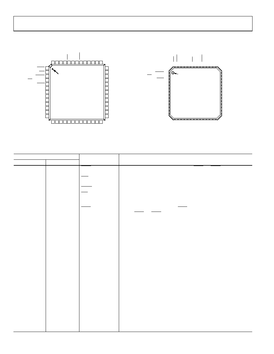
Figure 7. 52-Lead LQFP Pin Configuration
Figure 8. 56-Lead LFCSP Pin Configuration
Table 5. LQFP Pin Function Descriptions
Pin No.
Mnemonic
Description
LQFP
LFCSP
1
55
LDAC
Load DAC Logic Input (Active Low). See the BUSY and LDAC Functions
section for more information.
2
56
CLR
Asynchronous Clear Input (Level Sensitive, Active Low). See the Clear
Function section for more information.
3
1
RESET
Digital Reset Input.
4
2
BIN/2SCOMP
Data Format Digital Input. Connecting this pin to DGND selects offset binary.
Connecting this pin to logic 1 selects twos complement. This input has a weak
pull-down.
5
3
BUSY
Digital Input/Open-Drain Output. BUSY is open drain when it is an output.
See the BUSY and LDAC Functions section for more information.
6
4
GPIO
Digital I/O Pin. This pin can be configured as an input or output that can be
read or programmed high or low via the serial interface. When configured as
an input, it has a weak pull-down.
7
5
MON_OUT
Analog Multiplexer Output. Any DAC output, the MON_IN0 input, or the
MON_IN1 input can be switched to this output.
8, 32
6, 34
MON_IN0, MON_IN1
Analog Multiplexer Inputs. Can be switched to MON_OUT.
9, 10, 14, 24, 25,
26, 27, 30
7 to 11, 15, 16,
26 to 28, 31, 32
NC
No Connect.
11, 28
12, 29
VDD
Positive Analog Power Supply; +9 V to +16.5 V for specified performance.
These pins should be decoupled with 0.1 μF ceramic capacitors and 10 μF
capacitors.
12, 29
13, 30
VSS
Negative Analog Power Supply; 16.5 V to 8 V for specified performance.
These pins should be decoupled with 0.1 μF ceramic capacitors and 10 μF
capacitors.
13
14
VREF1
Reference Input for DAC 8 to DAC 15. This voltage is referred to AGND.
19
21
SIGGND1
Reference Ground for DAC 8 to DAC 15. VOUT8 to VOUT15 are referenced to
this voltage.
31
33
VREF0
Reference Input for DAC 0 to DAC 7. This voltage is referred to AGND.
33
35
TEMP_OUT
Provides an output voltage proportional to chip temperature. This is typically
1.46 V at 25°C with an output variation of 4.4 mV/°C.
34 to 37, 39 to
42, 15 to 18, 20
to 23
36 to 39, 41 to
44, 17 to 20, 22
to 25
VOUT0 to VOUT15
DAC Outputs. Buffered analog outputs for each of the 16 DAC channels. Each
analog output is capable of driving an output load of 10 kΩ to ground.
Typical output impedance of these amplifiers is 0.5 Ω.
相关PDF资料 |
PDF描述 |
|---|---|
| V300C2E50BF3 | CONVERTER MOD DC/DC 2V 50W |
| 0210490910 | CABLE JUMPER 1.25MM .178M 21POS |
| V24C5E125BL2 | CONVERTER MOD DC/DC 5V 125W |
| EVAL-AD5433EBZ | BOARD EVAL FOR AD5433 |
| HCC08DRES-S13 | CONN EDGECARD 16POS .100 EXTEND |
相关代理商/技术参数 |
参数描述 |
|---|---|
| EVAL-AD5361EBZ1 | 制造商:AD 制造商全称:Analog Devices 功能描述:16-Channel, 16-/14-Bit, Serial Input, Voltage-Output DAC |
| EVAL-AD5362EBZ | 功能描述:BOARD EVAL FOR AD5362 RoHS:是 类别:编程器,开发系统 >> 评估板 - 数模转换器 (DAC) 系列:- 产品培训模块:Lead (SnPb) Finish for COTS Obsolescence Mitigation Program 标准包装:1 系列:- DAC 的数量:4 位数:12 采样率(每秒):- 数据接口:串行,SPI? 设置时间:3µs DAC 型:电流/电压 工作温度:-40°C ~ 85°C 已供物品:板 已用 IC / 零件:MAX5581 |
| EVAL-AD5363EBZ | 功能描述:BOARD EVALUATION FOR AD5363 RoHS:是 类别:编程器,开发系统 >> 评估板 - 数模转换器 (DAC) 系列:- 产品培训模块:Lead (SnPb) Finish for COTS Obsolescence Mitigation Program 标准包装:1 系列:- DAC 的数量:4 位数:12 采样率(每秒):- 数据接口:串行,SPI? 设置时间:3µs DAC 型:电流/电压 工作温度:-40°C ~ 85°C 已供物品:板 已用 IC / 零件:MAX5581 |
| EVAL-AD5370EBZ | 功能描述:BOARD EVALUATION FOR AD5370 RoHS:是 类别:编程器,开发系统 >> 评估板 - 数模转换器 (DAC) 系列:- 产品培训模块:Lead (SnPb) Finish for COTS Obsolescence Mitigation Program 标准包装:1 系列:- DAC 的数量:4 位数:12 采样率(每秒):- 数据接口:串行,SPI? 设置时间:3µs DAC 型:电流/电压 工作温度:-40°C ~ 85°C 已供物品:板 已用 IC / 零件:MAX5581 |
| EVAL-AD5371EBZ | 功能描述:BOARD EVAL FOR AD5371 RoHS:是 类别:编程器,开发系统 >> 评估板 - 数模转换器 (DAC) 系列:- 产品培训模块:Lead (SnPb) Finish for COTS Obsolescence Mitigation Program 标准包装:1 系列:- DAC 的数量:4 位数:12 采样率(每秒):- 数据接口:串行,SPI? 设置时间:3µs DAC 型:电流/电压 工作温度:-40°C ~ 85°C 已供物品:板 已用 IC / 零件:MAX5581 |
发布紧急采购,3分钟左右您将得到回复。