- 您现在的位置:买卖IC网 > PDF目录17065 > EVAL-AD5379EBZ (Analog Devices Inc)BOARD EVALUATION FOR AD5379 PDF资料下载
参数资料
| 型号: | EVAL-AD5379EBZ |
| 厂商: | Analog Devices Inc |
| 文件页数: | 16/29页 |
| 文件大小: | 0K |
| 描述: | BOARD EVALUATION FOR AD5379 |
| 产品培训模块: | DAC Architectures |
| 标准包装: | 1 |
| DAC 的数量: | 40 |
| 位数: | 14 |
| 采样率(每秒): | 50k |
| 数据接口: | 串行,并联 |
| 设置时间: | 20µs |
| DAC 型: | 电压 |
| 工作温度: | -40°C ~ 85°C |
| 已供物品: | 板,CD |
| 已用 IC / 零件: | AD5379 |
| 相关产品: | AD5379ABCZ-ND - IC DAC 14BIT 40CHAN 108CSPBGA AD5379ABC-ND - IC DAC 14BIT 40CH 108-CSPBGA |
第1页第2页第3页第4页第5页第6页第7页第8页第9页第10页第11页第12页第13页第14页第15页当前第16页第17页第18页第19页第20页第21页第22页第23页第24页第25页第26页第27页第28页第29页
AD5379
Rev. B | Page 22 of 28
INTERFACES
The AD5379 contains a serial and a parallel interface. The
active interface is selected via the SER/PAR pin.
The AD5379 uses an internal FIFO memory to allow high
speed successive writes in both serial and parallel modes. The
user can continue writing new data to the AD5379 while write
instructions are being executed. The BUSY signal goes low while
instructions in the FIFO are being executed. Up to 120 successive
instructions can be written to the FIFO at maximum speed.
When the FIFO is full, additional writes to the AD5379 are
ignored.
To minimize both the power consumption of the device and
on-chip digital noise, the active interface powers up fully only
when the device is being written to, that is, on the falling edge
of WR or on the falling edge of SYNC.
All digital interfaces are 2.5 V LVTTL-compatible when
operating from a 2.7 V to 3.6 V VCC supply.
PARALLEL INTERFACE
A pull-down on the SER/PAR pin makes the parallel interface
the default. If using the parallel interface, the SER/PAR pin can
be left unconnected.
shows the timing diagram for a
parallel write to the AD5379. The parallel interface is controlled
by the following pins.
CS Pin
Active low device select pin.
WR Pin
On the rising edge of WR, with CS low, the address values at
Pin A7 to Pin A0 are latched, and data values at Pin DB13 to
Pin DB0 are loaded into the selected AD5379 input registers.
REG1, REG0 Pins
The REG1 and REG0 pins determine the destination register of
the data being written to the AD5379. See Table 11.
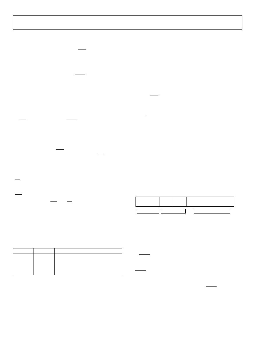
Table 11. Register Selection
REG1
REG0
Register Selected
1
Input data register (x1)
1
0
Offset register (c)
0
1
Gain register (m)
0
Special function register
DB13 to DB0 Pins
The AD5379 accepts a straight, 14-bit parallel word on Pin DB0
to Pin DB13, where Pin DB13 is the MSB and Pin DB0 is the
A7 to A0 Pins
Each of the 40 DAC channels can be individually addressed. In
addition, several channel groupings enable the user to simulta-
neously write the same data to multiple DAC channels. Address
Bits A7 to A4 are decoded to select one group or multiple
groups of registers. Address Bits A3 to A0 select one of ten
input data registers (x1), offset registers (c), or gain registers
(m). See Table 17.
SERIAL INTERFACE
The SER/PAR pin must be tied high to enable the serial inter-
face and disable the parallel interface. The serial interface is
controlled by five pins, as follows.
SYNC, DIN, SCLK
Standard 3-wire interface pins.
DCEN
Selects standalone mode or daisy-chain mode.
SDO
Data out pin for daisy-chain mode.
write to the AD5379 in standalone and daisy-chain modes,
respectively.
The 24-bit data word format for the serial interface is shown in
MSB
REG0
DB13–DB0
LSB
A7–A0
REG1
REGISTER DATA BITS
GROUP/CHANNEL
SELECT BITS
REGISTER SELECT
BITS
03165-021
Figure 21. Serial Data Format
Standalone Mode
By connecting the DCEN (daisy-chain enable) pin low,
standalone mode is enabled. The serial interface works with
both a continuous and a burst serial clock. The first falling edge
of SYNC starts the write cycle and resets a counter that counts
the number of serial clocks to ensure that the correct number of
bits is shifted into the serial shift register. Additional edges on
SYNC are ignored until 24 bits are shifted into the register.
Once 24 bits are shifted into the serial shift register, the SCLK is
ignored. In order for another serial transfer to take place, the
counter must be reset by the falling edge of SYNC.
相关PDF资料 |
PDF描述 |
|---|---|
| EVAL-AD5452EBZ | BOARD EVAL FOR AD5452 |
| EBA22DRMH | CONN EDGECARD 44POS .125 SQ WW |
| ACM03DRXN | CONN EDGECARD 6POS DIP .156 SLD |
| ESA06DTKT-S288 | CONN EDGECARD 12POS .125 EXTEND |
| RSM08DRUI | CONN EDGECARD 16POS DIP .156 SLD |
相关代理商/技术参数 |
参数描述 |
|---|---|
| EVAL-AD5380EB | 制造商:Analog Devices 功能描述:EVALUATION BOARD I.C. - Bulk |
| EVAL-AD5380EBZ | 功能描述:BOARD EVAL FOR AD5380 RoHS:是 类别:编程器,开发系统 >> 评估板 - 数模转换器 (DAC) 系列:- 产品培训模块:Lead (SnPb) Finish for COTS Obsolescence Mitigation Program 标准包装:1 系列:- DAC 的数量:4 位数:12 采样率(每秒):- 数据接口:串行,SPI? 设置时间:3µs DAC 型:电流/电压 工作温度:-40°C ~ 85°C 已供物品:板 已用 IC / 零件:MAX5581 |
| EVAL-AD5381EB | 制造商:Analog Devices 功能描述:EVAL KIT FOR 40-CH, 3V/5 V, SGL-SUPPLY, 12-BIT, VOLT OUTPUT - Bulk 制造商:Rochester Electronics LLC 功能描述: |
| EVAL-AD5382EB | 制造商:Analog Devices 功能描述:EVALUATION BOARD I.C. - Bulk 制造商:Rochester Electronics LLC 功能描述: |
| EVAL-AD5382EBZ | 功能描述:BOARD EVAL FOR AD5382 RoHS:是 类别:编程器,开发系统 >> 评估板 - 数模转换器 (DAC) 系列:- 产品培训模块:Lead (SnPb) Finish for COTS Obsolescence Mitigation Program 标准包装:1 系列:- DAC 的数量:4 位数:12 采样率(每秒):- 数据接口:串行,SPI? 设置时间:3µs DAC 型:电流/电压 工作温度:-40°C ~ 85°C 已供物品:板 已用 IC / 零件:MAX5581 |
发布紧急采购,3分钟左右您将得到回复。