- 您现在的位置:买卖IC网 > PDF目录17079 > EVAL-AD5421SDZ (Analog Devices Inc)BOARD EVAL FOR AD5421 PDF资料下载
参数资料
| 型号: | EVAL-AD5421SDZ |
| 厂商: | Analog Devices Inc |
| 文件页数: | 16/36页 |
| 文件大小: | 0K |
| 描述: | BOARD EVAL FOR AD5421 |
| 标准包装: | 1 |
| DAC 的数量: | 1 |
| 位数: | 16 |
| 数据接口: | 串行,SPI? |
| 设置时间: | 50µs |
| DAC 型: | 电压 |
| 工作温度: | -40°C ~ 105°C |
| 已供物品: | 板 |
| 已用 IC / 零件: | AD5421 |
第1页第2页第3页第4页第5页第6页第7页第8页第9页第10页第11页第12页第13页第14页第15页当前第16页第17页第18页第19页第20页第21页第22页第23页第24页第25页第26页第27页第28页第29页第30页第31页第32页第33页第34页第35页第36页
Data Sheet
AD5421
Rev. G | Page 23 of 36
ON-CHIP ADC
The AD5421 contains an on-chip ADC used to measure and
feed back to the fault register either the temperature of the die
or the voltage between the VLOOP and COM pins. The select ADC
input bit (Bit D8) of the control register selects the parameter
to be converted. A conversion is initiated with command byte
00001000 (necessary only if auto fault readback is disabled). This
command byte powers on the ADC and performs the conversion.
A read of the fault register returns the conversion result. If auto
readback of the fault register is required, the ADC must first be
powered up by setting the on-chip ADC bit (Bit D7) of the
control register.
Because the FAULT pin can go high for as long as 30 μs, care is
required when performing a die temperature measurement after
a readback of the VLOOP voltage. When switching from a VLOOP
measurement to a die temperature measurement, the FAULT
pin should not be read within 30 μs of switching, as a false
trigger may occur (fault register contents are unaffected).
VOLTAGE REGULATOR
The on-chip voltage regulator provides a regulated voltage out-
put to supply the AD5421 and the remainder of the transmitter
circuitry. The output voltage range is from 1.8 V to 12 V and is
selected by the states of three digital input pins (see Table 10).
The regulator output is accessed at the REGOUT pin.
Table 10. Setting the Voltage Regulator Output
REG_SEL2
REG_SEL1
REG_SEL0
Regulated Output
Voltage (V)
COM
1.8
COM
DVDD
2.5
COM
DVDD
COM
3.0
COM
DVDD
3.3
DVDD
COM
5.0
DVDD
COM
DVDD
9.0
DVDD
COM
12.0
LOOP CURRENT SLEW RATE CONTROL
The rate of change of the loop current can be controlled by
connecting an external capacitor between the CIN pin and
COM. This reduces the rate of change of the loop current.
The output resistance of the DAC (RDAC) together with the
CSLEW capacitor generate a time constant that determines the
response of the loop current (see Figure 45).
LOOP–
RDAC
V-TO-I
CIRCUITRY
CIN
CSLEW
09128-
052
Figure 45. Slew Capacitor Circuit
The resistance of the DAC is typically 15.22 k for the 4 mA
to 20 mA and 3.8 mA to 21 mA loop current ranges. The DAC
resistance changes to 16.11 k when the 3.2 mA to 24 mA loop
current range is selected.
The time constant of the circuit is expressed as
τ = RDAC × CSLEW
Taking five time constants as the required time to reach the final
value, CSLEW can be determined for a desired response time, t,
as follows:
DAC
SLEW
R
t
C
×
=
5
where:
t is the desired time for the output current to reach its final
value.
RDAC is the resistance of the DAC core, either 15.22 k or
16.11 k, depending on the selected loop current range.
For a response time of 5 ms,
nF
68
220
,
15
5
ms
5
≈
×
=
SLEW
C
For a response time of 10 ms,
nF
133
220
,
15
5
ms
10
≈
×
=
SLEW
C
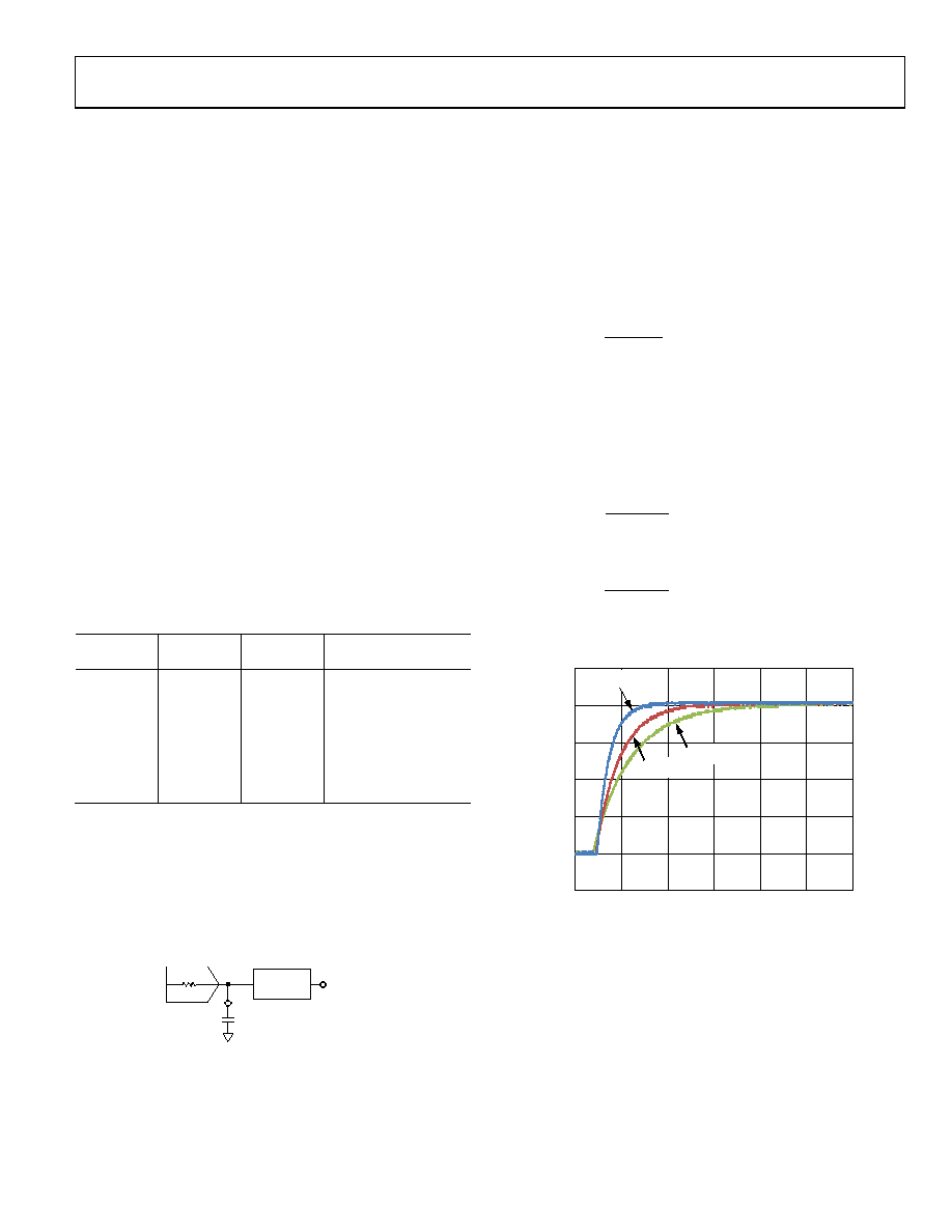
The responses for both of these configurations are shown
6
5
4
3
2
1
0
–2
22
18
14
10
6
2
VOLTA
GE
A
C
R
OS
S2
50
LOA
D
R
ES
IS
TOR
(V
)
TIME (ms)
CSLEW = 267nF
CSLEW = 133nF
CSLEW = 68nF
09128-
053
Figure 46. 4 mA to 20 mA Step with Slew Rate Control
The CIN pin can also be used as a coupling input for HART
FSK signaling. The HART signal must be ac-coupled to the CIN
input. The capacitor through which the HART signal is coupled
must be considered in the preceding calculations, where the
total capacitance is CSLEW + CHART. For more information, see
the HART Communications section.
相关PDF资料 |
PDF描述 |
|---|---|
| NR6028T150M | INDUCTOR 15UH 1.8A 20% SMD |
| SC53LC-6R8 | INDUCTOR SMD 6.8UH 1.51A 100KHZ |
| V48C2E50BL3 | CONVERTER MOD DC/DC 2V 50W |
| 0210490844 | CABLE JUMPER 1.25MM .178M 15POS |
| GBC05DREI-S734 | CONN EDGECARD 10POS .100 EYELET |
相关代理商/技术参数 |
参数描述 |
|---|---|
| EVAL-AD5422EBZ | 功能描述:BOARD EVAL FOR AD5422 RoHS:是 类别:编程器,开发系统 >> 评估板 - 数模转换器 (DAC) 系列:- 产品培训模块:Lead (SnPb) Finish for COTS Obsolescence Mitigation Program 标准包装:1 系列:- DAC 的数量:4 位数:12 采样率(每秒):- 数据接口:串行,SPI? 设置时间:3µs DAC 型:电流/电压 工作温度:-40°C ~ 85°C 已供物品:板 已用 IC / 零件:MAX5581 |
| EVAL-AD5422LFEBZ | 功能描述:BOARD EVAL FOR AD5422LFEBZ RoHS:否 类别:编程器,开发系统 >> 评估板 - 数模转换器 (DAC) 系列:* 产品培训模块:Lead (SnPb) Finish for COTS Obsolescence Mitigation Program 标准包装:1 系列:- DAC 的数量:4 位数:12 采样率(每秒):- 数据接口:串行,SPI? 设置时间:3µs DAC 型:电流/电压 工作温度:-40°C ~ 85°C 已供物品:板 已用 IC / 零件:MAX5581 |
| EVAL-AD5424EB | 制造商:Analog Devices 功能描述:EVALUATION BOARD I.C. - Bulk 制造商:Rochester Electronics LLC 功能描述: |
| EVAL-AD5424EBZ | 功能描述:BOARD EVALUATION FOR AD5424 RoHS:是 类别:编程器,开发系统 >> 评估板 - 数模转换器 (DAC) 系列:- 产品培训模块:Lead (SnPb) Finish for COTS Obsolescence Mitigation Program 标准包装:1 系列:- DAC 的数量:4 位数:12 采样率(每秒):- 数据接口:串行,SPI? 设置时间:3µs DAC 型:电流/电压 工作温度:-40°C ~ 85°C 已供物品:板 已用 IC / 零件:MAX5581 |
| EVAL-AD5425EB | 制造商:Analog Devices 功能描述:EVALUATION BOARD I.C. - Bulk |
发布紧急采购,3分钟左右您将得到回复。